Air gaps between conductive lines for reduced RC delay of integrated circuits

Inactive Publication Date: 2006-04-20
IBM CORP +1
View PDF7 Cites 12 Cited by
  • Summary
  • Abstract
  • Description
  • Claims
  • Application Information

AI Technical Summary

Benefits of technology

[0015] Advantages of preferred embodiment of the present invention include forming air gaps and/or highly porous dielectric material in critical areas, but not in non-critical areas, where the RC delay is not an issue. Because some regions of the workpiece do not have the air gaps or highly porous dielectric material di

Problems solved by technology

As the minimum line width on an integrated circuit becomes smaller, the active device density increases, and transistor switching speed decreases, while signal propagation delays in the interconnect system become limiting on the performance of the integrated circuit.
Thus, many large ultra-large scale i

Method used


Image

  • Air gaps between conductive lines for reduced RC delay of integrated circuits
  • Air gaps between conductive lines for reduced RC delay of integrated circuits
  • Air gaps between conductive lines for reduced RC delay of integrated circuits

Examples


Embodiment Construction

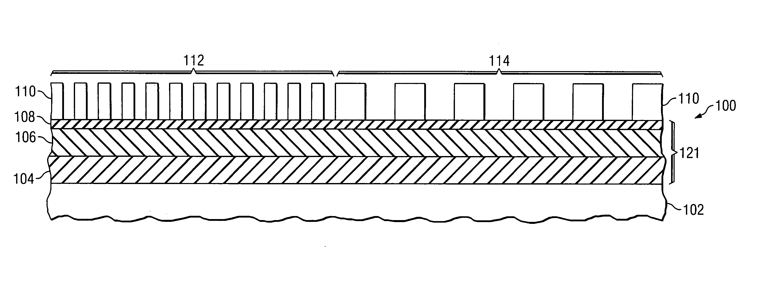
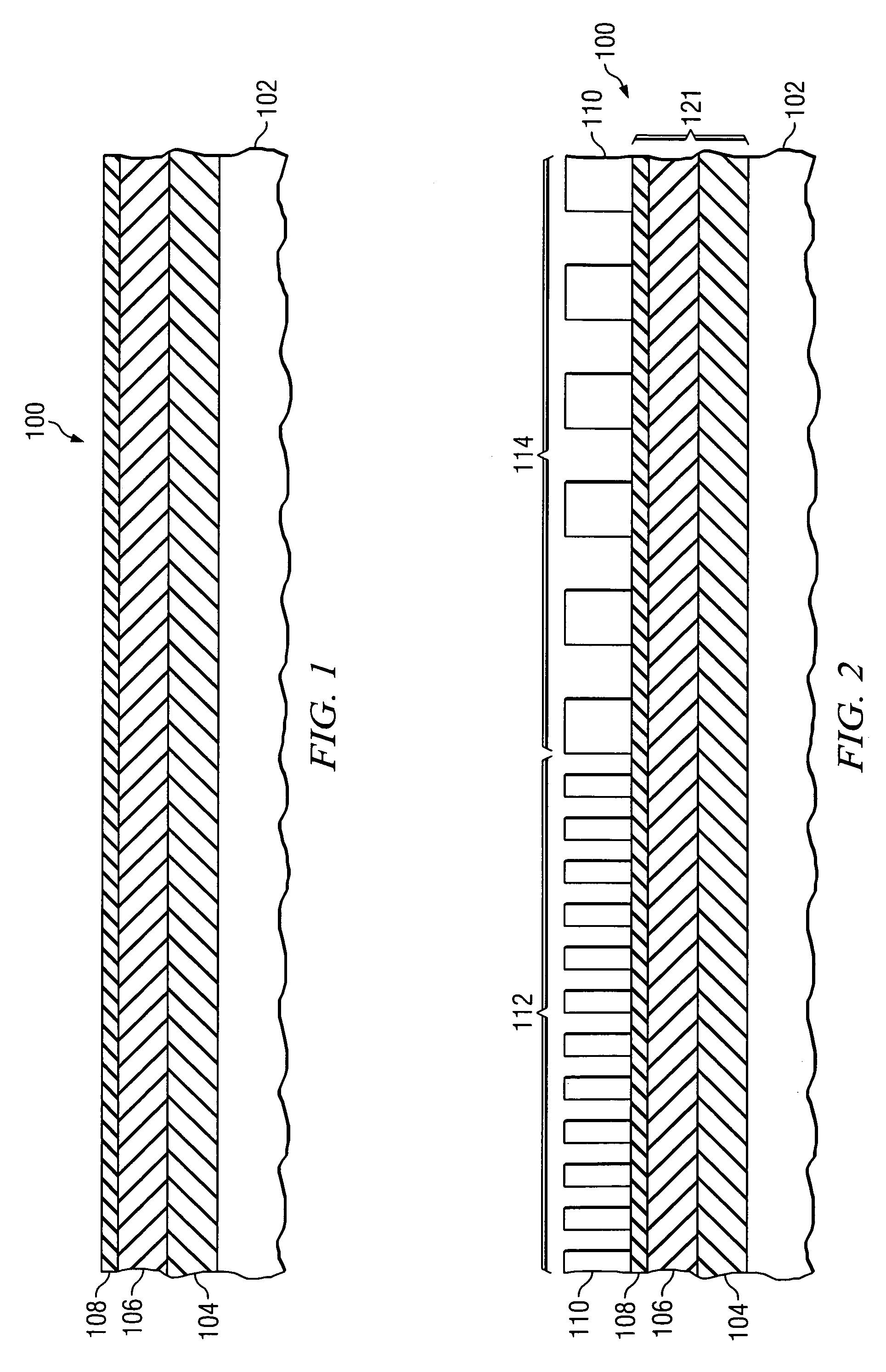
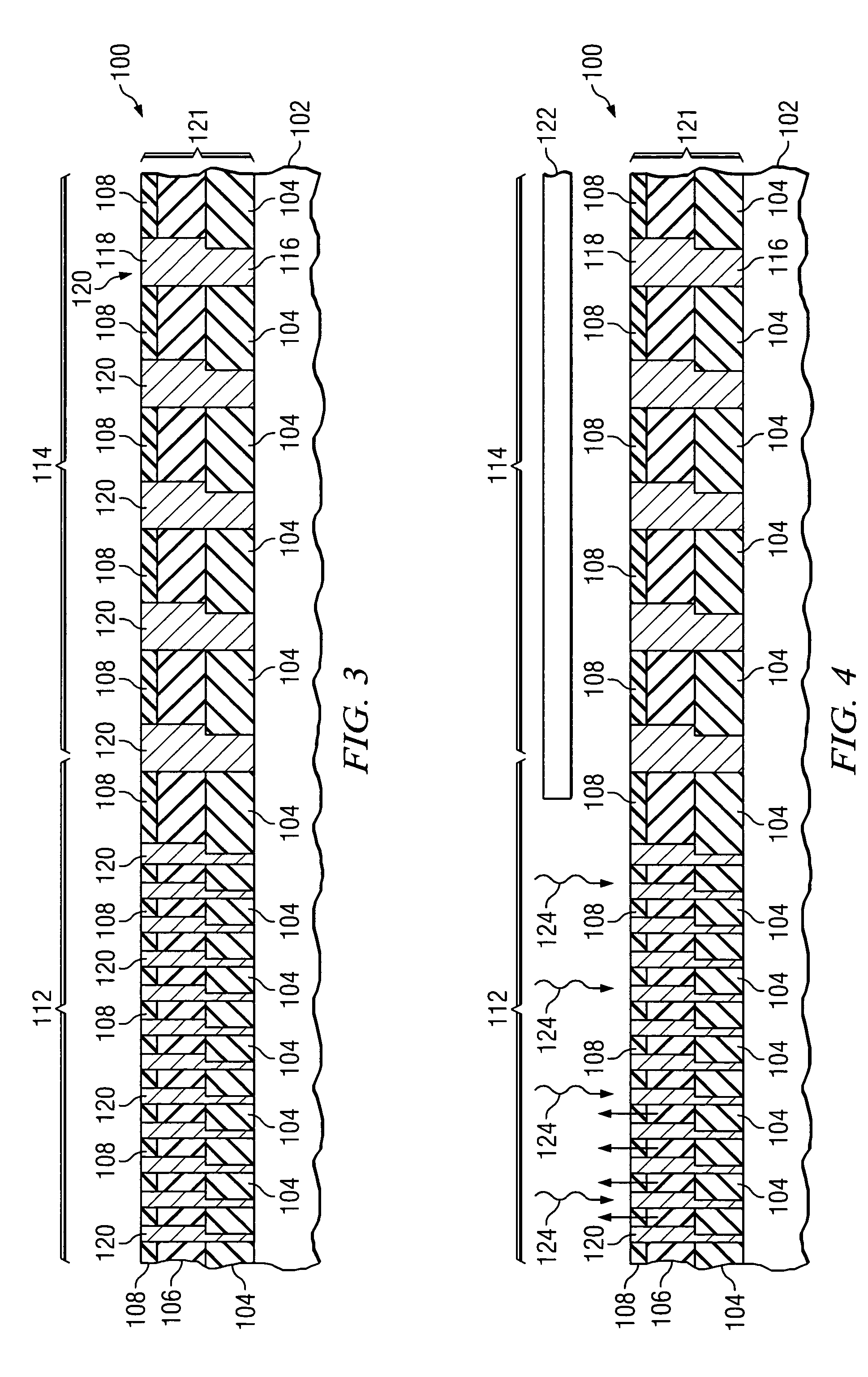
[0025] The making and using of the presently preferred embodiments are discussed in detail below. It should be appreciated, however, that the present invention provides many applicable inventive concepts that can be embodied in a wide variety of specific contexts. The specific embodiments discussed are merely illustrative of specific ways to make and use the invention, and do not limit the scope of the invention.

[0026] The present invention will be described with respect to preferred embodiments in a specific context, namely semiconductor device having multiple layers of interconnect. The invention may also be applied, however, to semiconductor devices having a single layer of interconnect, for example.

[0027] The capacitance C in the RC delay of BEOL interconnect may be lowered by the use of low-k materials. For example, silicon dioxide (SiO2), commonly used as an interconnect insulating material in the past, has a dielectric constant k of about 4.1 or 4.2. A dense low-k material ...


PUM


Abstract

Methods of forming air gaps or porous dielectric materials between interconnects of integrated circuits and structures thereof. Air gaps or highly porous dielectric material having a dielectric constant of close to or equal to 1.0 are formed in a first region but not a second region of an interconnect layer. The air gaps or highly porous dielectric material are formed by depositing a first insulating material comprising an energy-sensitive material over a workpiece, depositing a second insulating material over the first insulating material, and exposing the workpiece to energy. At least a portion of the first insulating material in the first region is removed through the second insulating material. Structurally stable insulating material is disposed between conductive lines in the second region of the workpiece, providing mechanical strength for the integrated circuit.

Description

TECHNICAL FIELD [0001] The present invention relates generally to the fabrication of semiconductor devices, and more particularly to the formation of insulating materials of interconnect layers. BACKGROUND [0002] Semiconductor devices are used in a variety of electronic applications, such as computers, cellular phones, personal computing devices, and many other applications. Home, industrial, and automotive devices that in the past comprised only mechanical components now have electronic parts that require semiconductor devices, for example. [0003] Semiconductor devices typically include several layers of insulating, conductive and semiconductive materials that are patterned to form integrated circuits. There may be a plurality of transistors, memory devices, switches, conductive lines, diodes, capacitors, logic circuits, and other electronic components formed on a single die or chip. Semiconductor technology has experienced a trend towards miniaturization, to meet the demands of pr...

Claims


Application Information

Patent Timeline
IPC IPC(8): H01L29/04
CPCH01L21/7682H01L23/5222H01L23/5329H01L2924/0002H01L2924/00H01L2221/1047
Inventor KNORR, ANDREASKASTENMEIER, BERNDMOUMEN, NAIM
Owner IBM CORP
Why Eureka
Try Eureka