Piezoelectic device

Active Publication Date: 2006-04-20
SEIKO EPSON CORP
View PDF3 Cites 24 Cited by
  • Summary
  • Abstract
  • Description
  • Claims
  • Application Information

AI Technical Summary

Benefits of technology

[0008] A piezoelectric device according to the invention is characterized in that an IC chip is mounted on an inner bottom surface of a package, and a piezoelectric vibrating reed is electrically and mechanically connected onto a TAB tape in which a lead is provided on a surface of a resin tape. The TAB tape to which the piezoelectric vibrating reed has been joined is mounted in the package, whereby the piezoelectric vibrating reed is arranged above the IC chip. In this case, the IC chip includes at least a circuit for driving the piezoelectric vibrating reed, and a circuit for detecting a signal outputted from the piezoelectric vibrating reed. Since the piezoelectric vibrating reed can be arranged above the IC chip, the plane size of the piezoelectric device can be miniaturized. Therefore, the space where the piezoelectric device is mounted on a mounting substrate can be reduced.
[0009] Further, the piezoelectric device is characterized in that the TAB tape has a device hole in its center, and the lead is protruded inward of the device hole. The leading end portion of the lead and a connection electrode provided for the piezoelectric vibrating reed are electrically and mechanically connected. Even if the device hole is provided in the center portion of the TAB tape, because the IC chip is mounted on the inner bottom surface of the package, the piezoelectric vibrating reed can be arranged above the IC chip so that the plane size of the piezoelectric device can be miniaturized. Further, since the TAB tape is joined to the piezoelectric vibrating reed, the elements for calculation can be reduced when the resonance design of the TAB tape is performed. As such, the resonance design can be performed exactly.
[0010] Further, the piezoelectric device is characterized in that the piezoelectric vibrating reed has in its center a base portion on which the connection electrode is formed. A drive arm and a detection arm for detecting an angular velocity are

Problems solved by technology

However, when an electronic apparatus on which the piezoelectric device is mounted is minaturized, it is necessary to reduce the thickness and the plane size of the piezoelectric device.
Therefore, the plane size of the piezoelectric device becomes large and the miniaturization cannot be achieved, so that the mounted space of the piezoelectric device becomes large.
Further, if the gy

Method used


Image

  • Piezoelectic device
  • Piezoelectic device
  • Piezoelectic device

Examples


Example

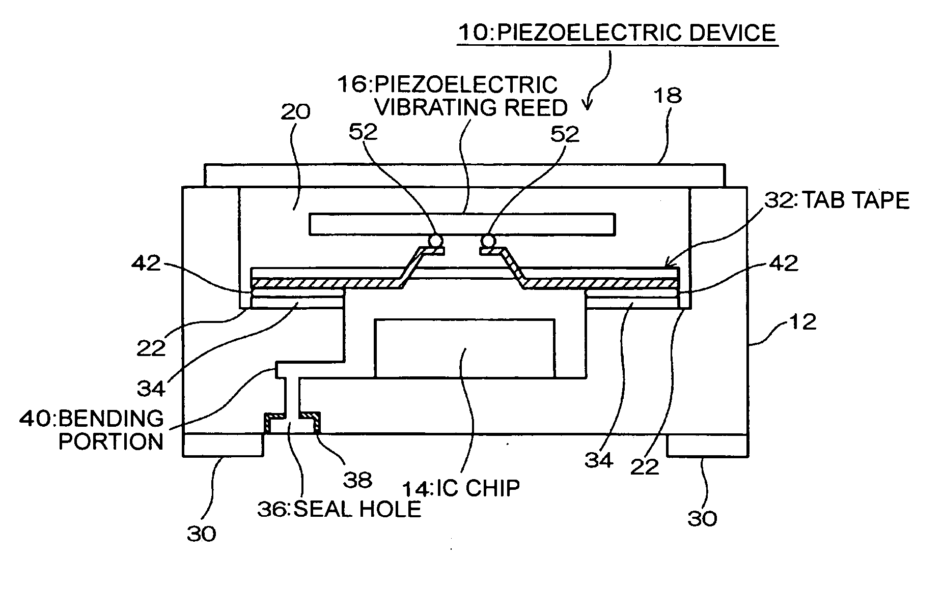
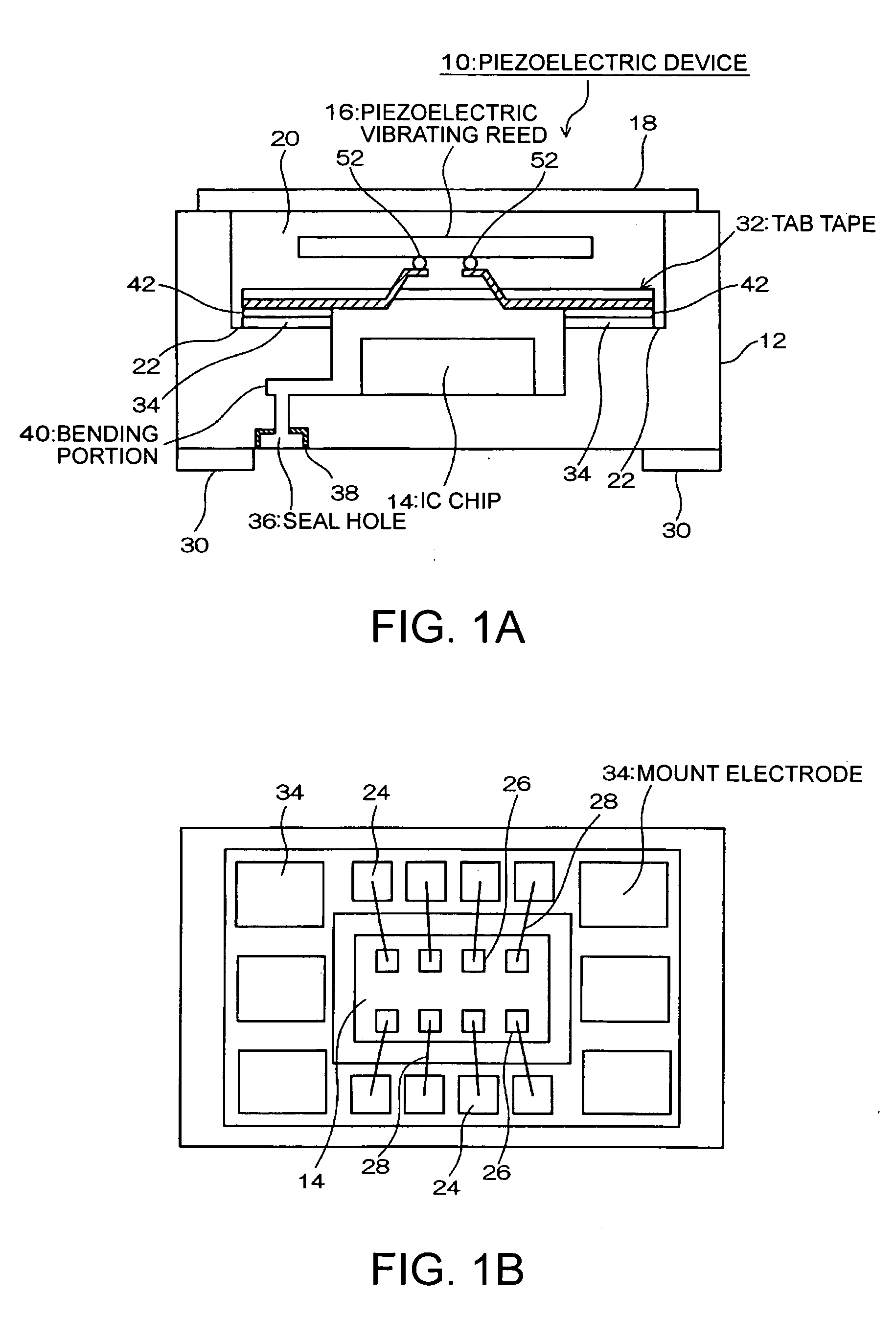
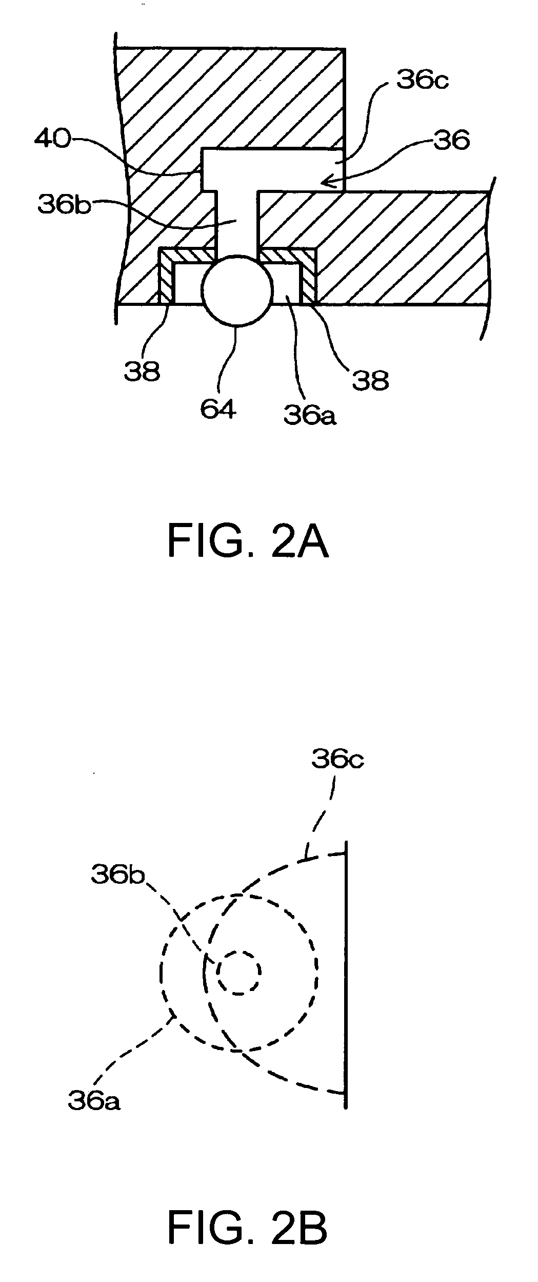
[0022] A piezoelectric device according to the present invention will now be described below. FIG. 1 is an explanatory view of a piezoelectric device, in which FIG. 1(a) is a schematic sectional view, and FIG. 1(b) is a schematic plan view in which a lid and a TAB tape are removed. FIG. 2 is an explanatory view of a seal hole, in which FIG. 2(a) is a schematic sectional view, and FIG. 2(b) is a schematic plan view. FIG. 3 is an explanatory view of the TAB tape, in which FIG. 3(a) is a schematic plan view, and FIG. 3(b) is a sectional view taken along a line A-A of FIG. 3(a). FIG. 4 is an explanatory view of a piezoelectric vibrating reed. In the piezoelectric device 10, an integrated circuit (IC) chip 14 is mounted on an inner bottom surface of a package base 12, a TAB tape 32 is mounted to which a piezoelectric vibrating reed 16 is electrically and mechanically connected, the piezoelectric vibrating reed 16 is arranged above the IC chip 14, and a lid 18 is joined onto an upper surf...


PUM


Abstract

A piezoelectric device including an IC chip mounted on an inner bottom surface of a package, and a piezoelectric vibrating reed electrically and mechanically connected onto a TAB tape in which a lead is provided on a surface of a resin tape. The TAB tape to which the piezoelectric vibrating reed has been joined is mounted in the package, whereby the piezoelectric vibrating reed is arranged above the IC chip.

Description

TECHNICAL FIELD [0001] The present invention relates to a piezoelectric device, and particularly to a piezoelectric device provided with a piezoelectric vibrating reed and an IC chip that are mounted on a TAB tape. BACKGROUND ART [0002] As piezoelectric devices go, there are a gyro sensor for detecting an angular velocity, a piezoelectric vibrator and a piezoelectric oscillator that output a desired oscillation frequency, and a filter that selects a desired frequency band. A piezoelectric oscillator includes a package base having a recess portion therein. Onto this recess portion, a TAB tape is mounted, in which a wiring pattern to which an IC chip and a piezoelectric vibrating reed are connected is provided on the surface of an insulation tape. This TAB tape is constructed so that a window portion is provided for the insulation tape. A part of the wiring pattern is bent upward through this window portion. Further, on the lower surface of the TAB tape, the IC chip is mounted. The pi...

Claims


Application Information

Patent Timeline
IPC IPC(8): H01L41/053G01C19/56G01C19/5628H01L41/08H01L41/09H01L41/22H01L41/23H01L41/311H03B5/32H03H3/02
CPCG01C19/56H03H9/0547H03H9/1021H10N30/20
Inventor KINOSHITA, YUSUKE
Owner SEIKO EPSON CORP
Why Eureka
Try Eureka