Test system for device characterization

Inactive Publication Date: 2006-04-20
FREESCALE SEMICON INC
View PDF13 Cites 12 Cited by
  • Summary
  • Abstract
  • Description
  • Claims
  • Application Information

AI Technical Summary

Problems solved by technology

One problem with such systems is that the circuitry coupling the external connections to the device under test can not be varied with respect to the different frequencies.
Accordingly, such a fixture can not be used to perform device characterizations that are optimized at different frequencies.

Method used


Image

  • Test system for device characterization
  • Test system for device characterization
  • Test system for device characterization

Examples


Embodiment Construction

[0018] The following sets forth a detailed description of a mode for carrying out the invention. The description is intended to be illustrative of the invention and should not be taken to be limiting.

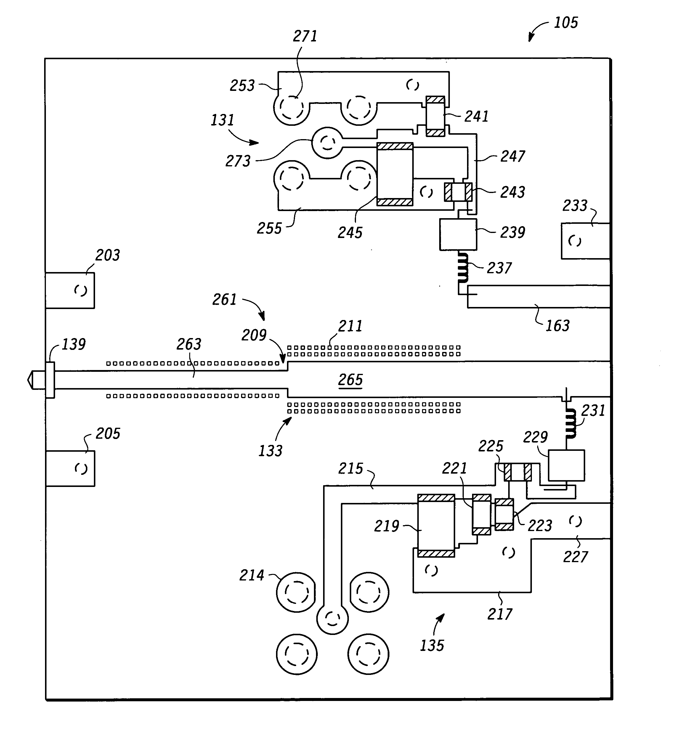
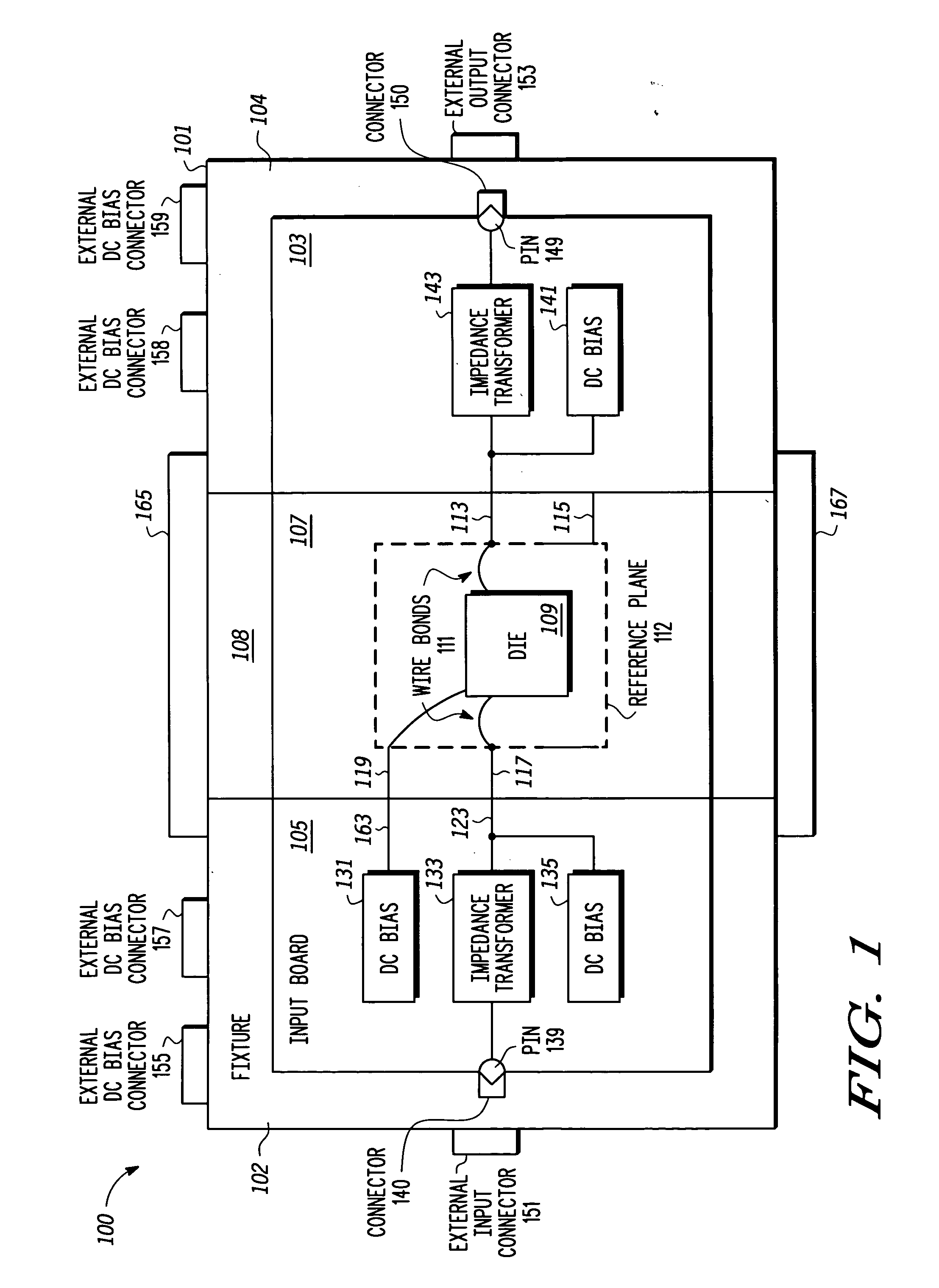
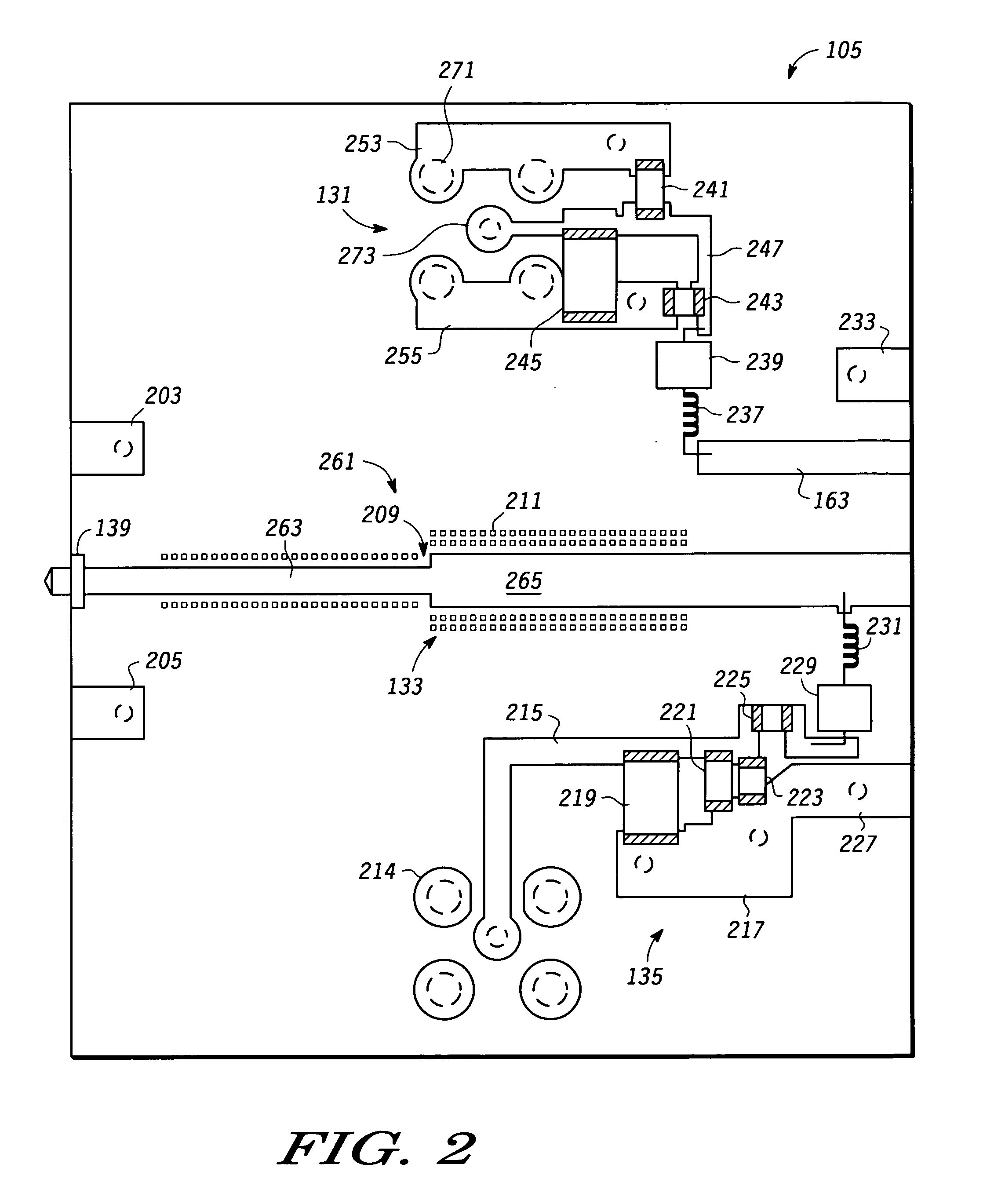
[0019]FIG. 1 is a top view of a test system 100 for measuring characteristics (e.g. RF characteristics) of a device under test. In the embodiment shown, the device under test is implemented in semiconductor die 109, but may be in other configurations in other embodiments. In one embodiment, die 109 includes an RF device such as e.g. a 7200 micron squared Hetro-Junction Bipolar transistor, but may include other RF devices in other embodiments such as e.g. Emode, GaAsfet, pHempt, Silicon HBT, and RF-CMOS transistors.

[0020] Die 109 is attached to a carrier 107. Carrier 107 includes signal traces 117, 113, 115, and 119, which in one embodiment are metal traces on a ceramic substrate. Carrier 107 is removably attached (e.g. with screws) to a carrier midsection 108 of test system 100.

[0021...


PUM


Abstract

Device characterization performed with a test system including a fixture and multiple frequency dependent test boards. In one embodiment, testing is performed with multiple sets of input and output test boards wherein each set is frequency dependent at different frequencies. In some examples, the test board includes an impedance transformer that is a quarter wave length of the fundamental frequency (f0) of a frequency of which the board is dependent. In some examples, S-parameters and load pull measurements are obtained for the device under test with the test boards at different frequencies.

Description

BACKGROUND OF THE INVENTION [0001] 1. Field of the Invention [0002] This invention relates in general to testing systems for electronic device characterization. [0003] 2. Description of the Related Art [0004] Testing systems include fixtures for performing tests for electronic device characterization. Such a device characterization can be used to design and build integrated circuits with the device. [0005] Some previous test systems utilized fixtures with DC bias circuitry and frequency specific circuitry for a particular frequency built on the fixture between external connectors. A carrier with a package could then be attached to the fixture. Examples of such systems include the MAURY MICROWAVE MT950 sold by the MAURY CORP. One problem with such systems is that the circuitry coupling the external connections to the device under test can not be varied with respect to the different frequencies. Accordingly, such a fixture can not be used to perform device characterizations that are o...

Claims


Application Information

Patent Timeline
IPC IPC(8): G01R31/02
CPCG01R27/28G01R31/2837
Inventor MAJERUS, MICHAEL E.KNAPPENBERGER, WILLIAM P.
Owner FREESCALE SEMICON INC
Why Eureka
Try Eureka