Semiconductor device formed on insulating layer and method of manufacturing the same

a technology of semiconductor devices and insulating layers, applied in the direction of semiconductor devices, electrical devices, transistors, etc., can solve the problems of affecting the manufacturing process, the transistor is turned, and the disadvantage of the proposed manufacturing process, and achieve the effect of easy manufacturing of semiconductor devices

Inactive Publication Date: 2006-04-27
RENESAS TECH CORP
View PDF10 Cites 10 Cited by
  • Summary
  • Abstract
  • Description
  • Claims
  • Application Information

AI Technical Summary

Benefits of technology

[0024] Another object of the invention is to provide a semiconductor device which can prevent concentration of an electric field at the vicinity of a side surface of an SOI layer.
[0081] Thereby, it is possible to prevent movement of oxidant to the lower surfaces of the first and second semiconductor layers when oxidizing the first and second semiconductor layers, and the nitride film reduces a difference in level between the first and second insulating layers.

Problems solved by technology

Therefore, a disadvantage occurs in connection with subthreshold characteristics of a regular MOS transistor formed at SOI layer 3.
More specifically, since the threshold voltage of parasitic transistor lowers as already described, such a disadvantage is caused that the parasitic transistor is turned on by a voltage lower than the threshold voltage of the regular transistor.
However, the proposed manufacturing process may suffer from the following problem.
Thereby, the subthreshold characteristics of regular transistor are adversely affected.
This lowers the threshold voltage of parasitic transistor, and thus the subthreshold characteristics of regular transistor are adversely affected.
As described above, various problems arise in the manufacturing process proposed in the prior art, and consequently, it is difficult to improve the subthreshold characteristics of regular transistor.

Method used


Image

  • Semiconductor device formed on insulating layer and method of manufacturing the same
  • Semiconductor device formed on insulating layer and method of manufacturing the same
  • Semiconductor device formed on insulating layer and method of manufacturing the same

Examples


first embodiment

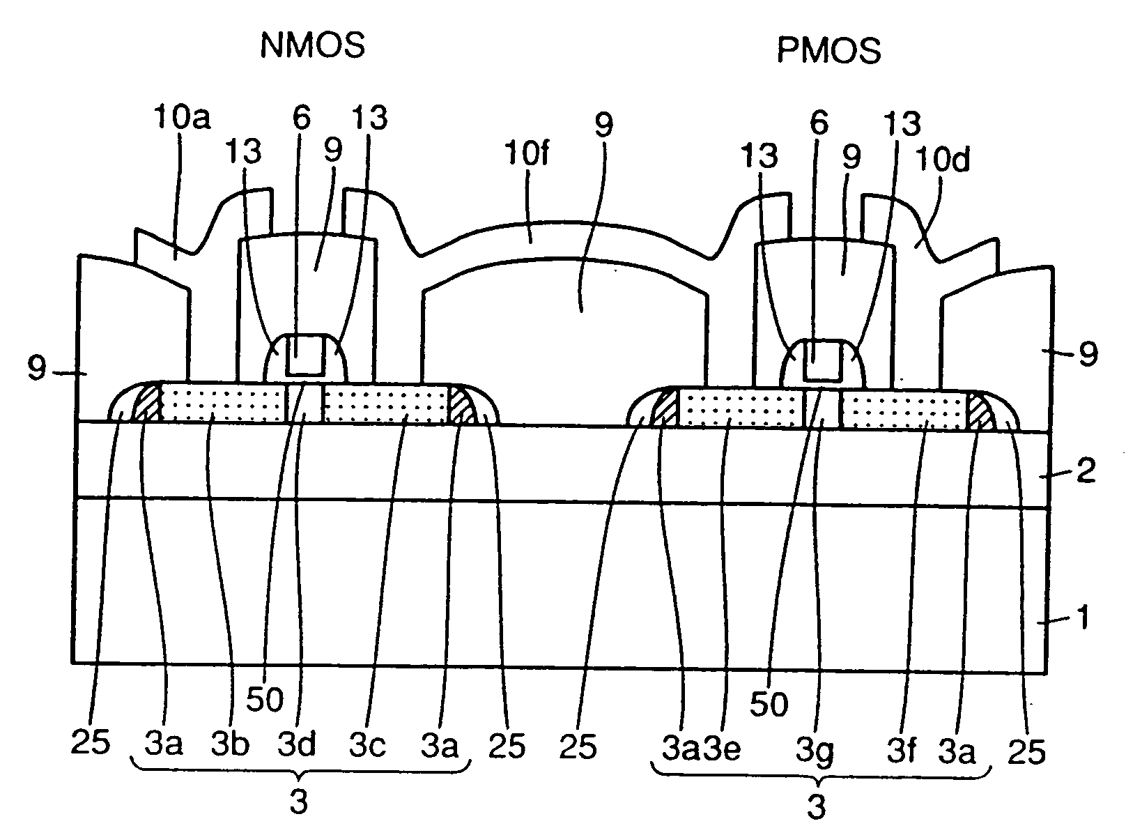
[0151] In this first embodiment, upper side portions of each SOI layer 3 are rounded. Thereby, it is possible to prevent concentration of an electric field at the upper side portions of SOI layers 3. Consequently, lowering of a threshold voltage of a parasitic transistor can be prevented, which suppresses turn-on of the parasitic transistor. As a result, subthreshold characteristics of a regular MOS transistor are prevented from being adversely affected by the parasitic transistor. The lower portion of the side surface of SOI layer 3 extends substantially perpendicularly to a main surface of the buried oxide film 2, so that such a structure can be prevented that a thin portion is formed at the lower side portion of SOI layer 3. Thereby, it is possible to prevent lowering of the threshold voltage of parasitic transistor which may be caused by reduction of the thickness of SOI layer 3 at the vicinity of its side surface.

[0152] In this first embodiment, buried oxide film 2 is provided ...

second embodiment

[0170] Referring to FIGS. 24 to 32, a process of manufacturing the semiconductor device of the second embodiment will be described below.

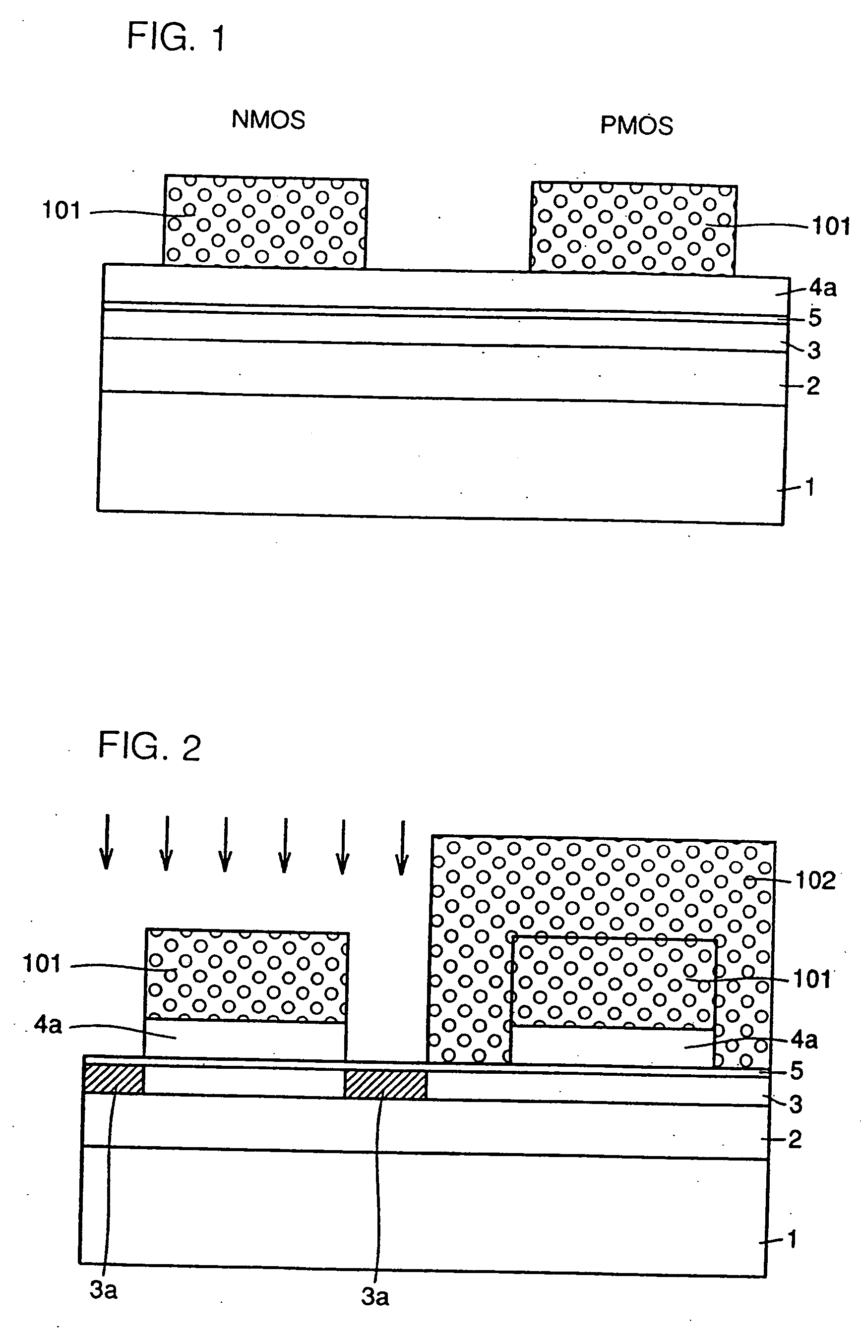
[0171] Referring first to FIG. 24, buried oxide film 2 is formed on silicon substrate 1, and then SOI layer 3 is formed on buried oxide film 2. Oxide film 5 having a thickness of about 100 Å is formed on SOI layer 3. Oxide film 5 may be formed by the CVD method under the temperature condition of about 800° C., or by oxidizing the surface of SOI layer 3 under the temperature condition of about 800° C. Nitride film 4a having a thickness of about 1000 Å is formed on oxide film 5 by the CVD method under the temperature condition of about 700° C. A resist 101 is formed at predetermined regions on nitride film 4a. Using resist 101 as a mask, nitride film 4a is etched to pattern the same.

[0172] Then, resist 102 covering the PMOS region is formed as shown in FIG. 25. Using resists 102 and 101 as a mask, boron ions (B+) are implanted into SOI layer 3 at th...

fourth embodiment

[0178] Referring to FIGS. 47 and 48, a semiconductor device of a fourth embodiment is provided with thermal oxidation films 5a covering side surfaces of SOI layer 3. There are formed oxide films 16 which are in contact with side surfaces of thermal oxidation films 5a and cover end surfaces of concavities 2b in buried oxide film 2. Thereby, it is possible to prevent such a disadvantage that gate electrode 6 extends up to the lower surface of SOI layer 3 due to formation of gate electrode 6 at the end of concavity 2b during the manufacturing process. As a result, it is possible to prevent concentration of an electric field which may be caused by the above extension of gate electrode 6.

[0179] Referring to FIGS. 40 to 47, a process of manufacturing the semiconductor device of the fourth embodiment will be described below. Referring to FIG. 40, buried oxide film 2 is formed on silicon substrate 1, and then SOI layer 3 is formed on buried oxide film 2. Oxide film 5 is formed on SOI layer ...


PUM


Abstract

In a semiconductor device having an SOI structure and a method of manufacturing the same, influence by a parasitic transistor can be prevented, and no disadvantage is caused in connection with a manufacturing process. In this semiconductor device, an upper side portion of a semiconductor layer is rounded. Thereby, concentration of an electric field at the upper side portion of the semiconductor layer can be prevented. As a result, lowering of a threshold voltage of a parasitic transistor can be prevented, so that the parasitic transistor does not adversely affect subthreshold characteristics of a regular transistor. Owing to provision of a concavity of a U-shaped section, generation of etching residue can be prevented when etching a gate electrode for patterning the same. Thereby, a disadvantage is not caused in connection with the manufacturing process.

Description

BACKGROUND OF THE INVENTION [0001] 1. Field of the Invention [0002] The present invention relates in general to a semiconductor device and a method of manufacturing the same, and in particular to a semiconductor device formed on an insulating layer and a method of manufacturing the same. [0003] 2. Description of the Background Art [0004] In order to improve the performance of semiconductor devices, there have been developed semiconductor devices in which circuit elements are isolated by dielectrics and a floating capacitance is small. For forming transistors on a thin silicon film on an insulating film, which will be referred to as an SOI (Silicon On Insulation) layer, an MESA isolating method is used for isolating the transistors from each other. According to this MESA isolating method, the isolated transistors are formed at completely isolated or insular SOI layers, respectively. This brings about many advantages such as prevention of influence of latch-up between adjacent transis...

Claims


Application Information

Patent Timeline
Patent Type & Authority Applications(United States)
IPC IPC(8): H01L29/08H01L29/04H01L27/12H01L27/14H01L21/764H01L21/265H01L21/336H01L21/76H01L21/762H01L21/8238H01L21/84H01L27/08H01L27/092H01L29/786
CPCH01L21/26586H01L21/76297H01L21/764H01L21/84H01L27/1203H01L29/66772H01L29/78606H01L29/78612H01L29/78633H01L29/78654
Inventor IWAMATSU, TOSHIAKIYAMAGUCHI, YASUOMAEDA, SHIGENOBUMIYAMOTO, SHOICHIFURUKAWA, AKIHIKOINOUE, YASUO
Owner RENESAS TECH CORP
Why Eureka
Try Eureka