Image sensor assembly and method for fabricating the same
a technology of image sensor and assembly method, which is applied in the direction of radiation control devices, semiconductor devices, semiconductor/solid-state device details, etc., can solve the problems of difficult to fabricate traces on the double layer and side of glass substrate, image sensor chip lack of protection, and high fabrication cost of glass substrate. achieve the effect of reducing the overall package thickness
- Summary
- Abstract
- Description
- Claims
- Application Information
AI Technical Summary
Benefits of technology
Problems solved by technology
Method used
Image
Examples
first embodiment
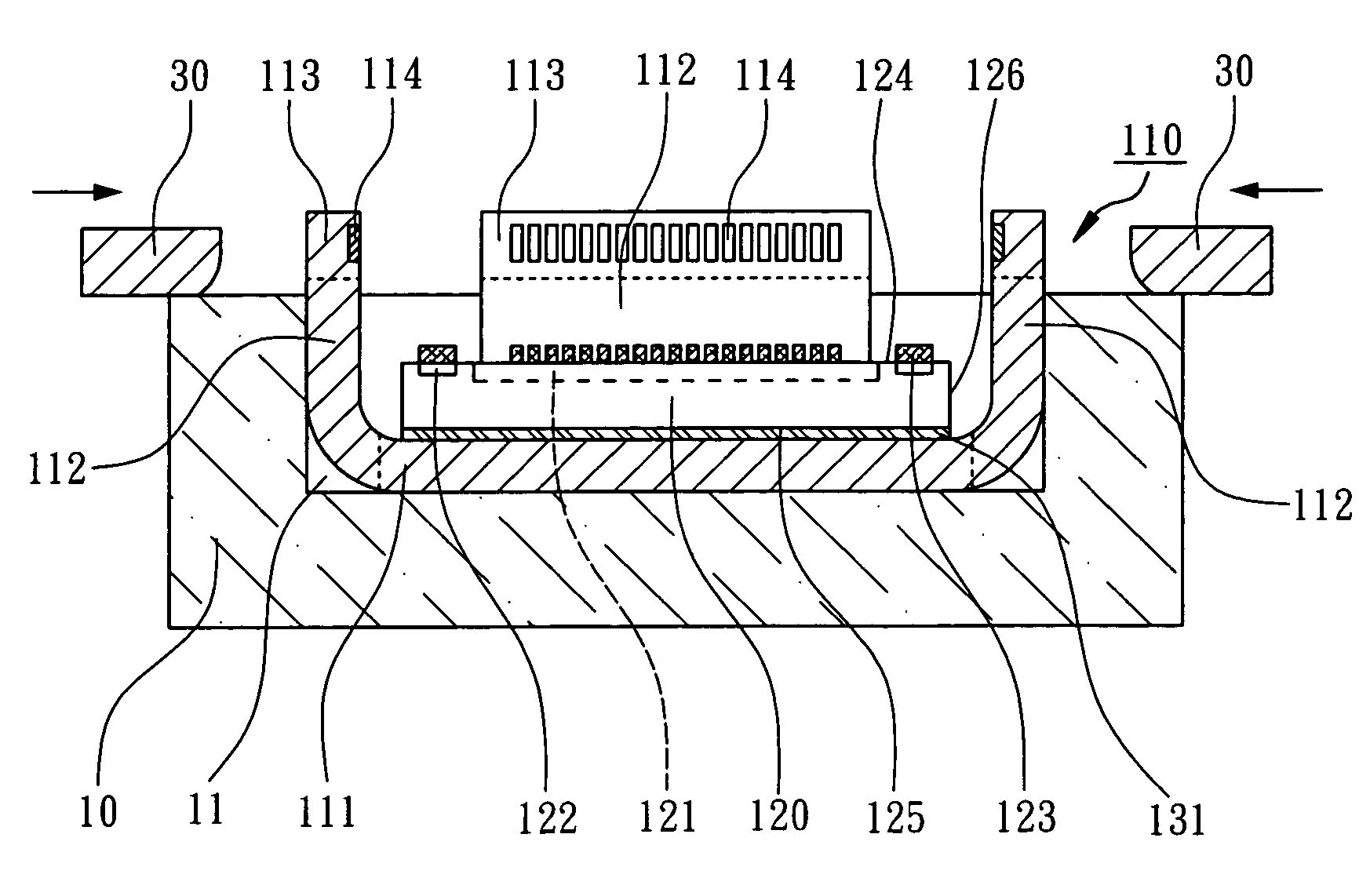
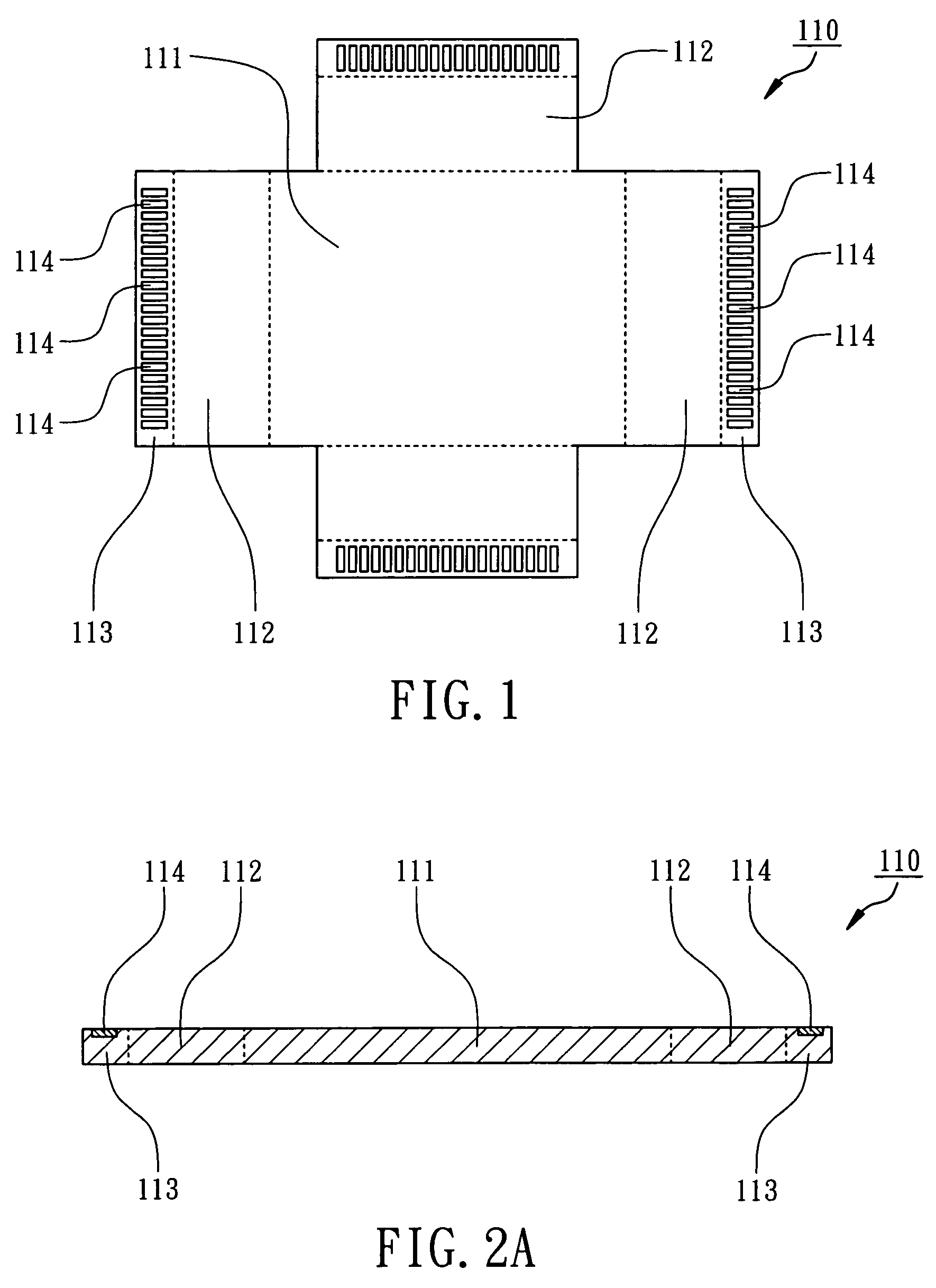
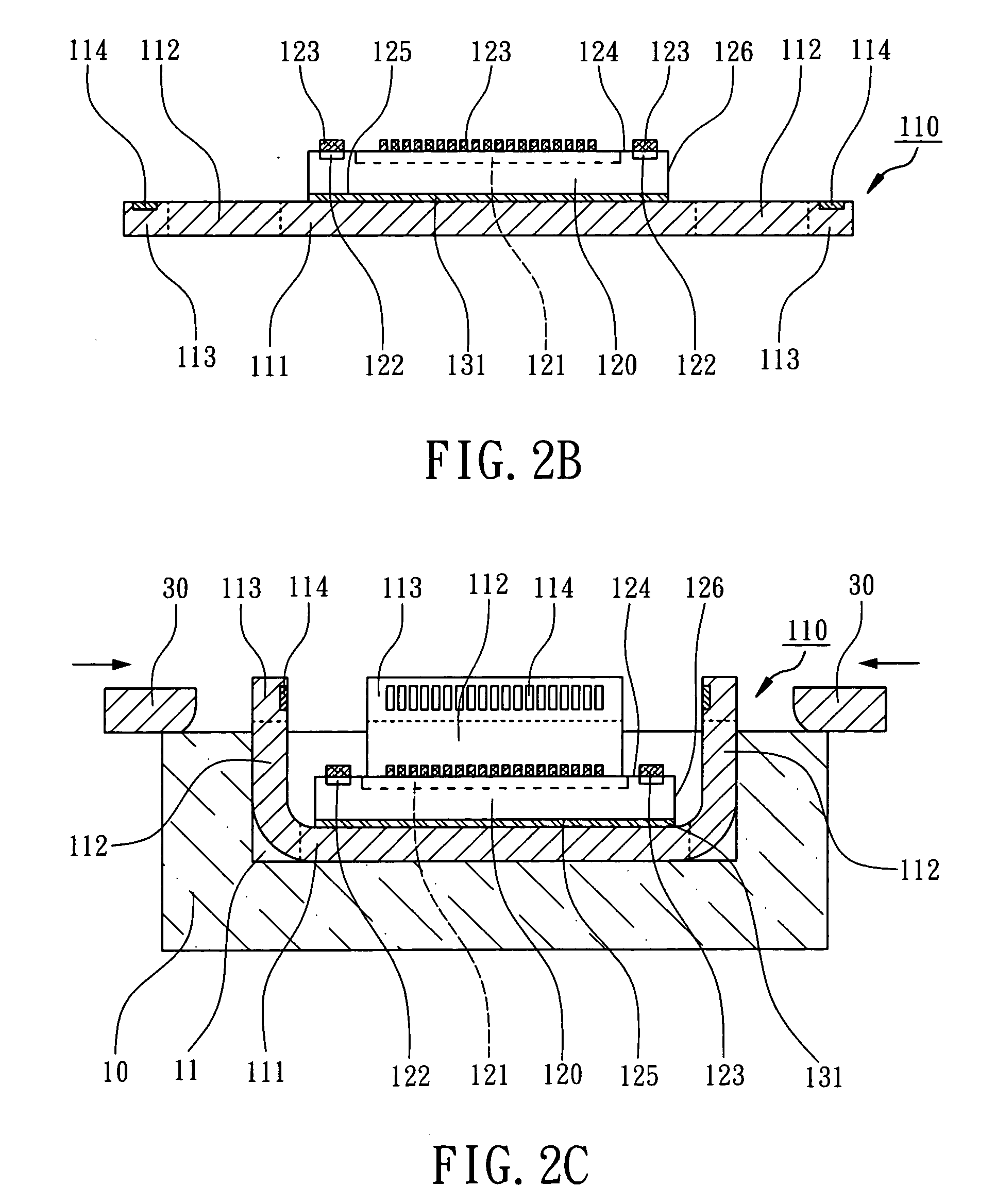
[0011] According to the present invention, FIG. 1 shows a flexible circuit for an image sensor assembly, FIG. 2A to 2F show the flexible circuit during assembling processes, especially FIG. 2F shows the cross-sectional view of the image sensor assembly. The image sensor assembly mainly comprises a flexible circuit 110 and an image sensor chip 120. As shown in FIGS. 1 and 2A, the flexible circuit 110 has a die-attached portion 111, a plurality of bendable portions 112 and a plurality of bonding portions 113 where the bendable portions 112 are extended from the die-attached portion 111 and are connected to the bonding portions 113 respectively. The flexible circuit 110 which is made of a polyimide (PI) film with a thickness not greater than 0.2 mm and has at least a wiring layer. A plurality of inner leads 114 are formed on the bonding portions 113 where the inner leads 114 are made of copper metal foil, preferably, a nickel / gold layer is disposed on the inner leads 114 (not shown in ...
second embodiment
[0018] According to the present invention, FIG. 3 shows another flexible circuit for an image sensor assembly, FIG. 4A to 4E show the flexible circuit during assembling processes, especially FIG. 4E shows the cross-sectional view of the image sensor assembly. The image sensor assembly mainly comprises a flexible circuit 210 and an image sensor chip 220. As shown in FIGS. 3 and 4A, the flexible circuit 210 has a die-attached portion 211, a plurality of bendable portions 212, and a plurality of bonding portions 213 where the bendable portions 212 are extended from the die-attached portion 211 and are connected to the bonding portions 213. A plurality of inner leads 214 are formed on the bonding portions 213. One bonding portion 213a of the bonding portions 213 has an opening 215. The opening 215 is aligned with a sensing area 221 of the image sensor chip 220 after thermocompression bonding the bonding portions 213 to the image sensor chip 220 (as shown in FIG. 4E). In this embodiment,...
PUM
 Abstract
Description
Claims
Application Information


