Desiccant film in top-emitting OLED

a technology of top-emitting oled and desiccant film, which is applied in the direction of discharge tube luminescnet screen, semiconductor/solid-state device details, etc., can solve the problems of inability to use in many applications, slow water absorption of calcium oxide and calcium chloride desiccants, and inability to handle such particulate materials, etc., to reduce the formation of aggregates, improve the effect of device performance and long li

Inactive Publication Date: 2006-04-27
EASTMAN KODAK CO
View PDF15 Cites 90 Cited by
  • Summary
  • Abstract
  • Description
  • Claims
  • Application Information

AI Technical Summary

Benefits of technology

[0014] The invention provides a top-emitting OLED device that is protected from moisture thereby achieving longer lifetime and excellent device performance.
[0015] One advantage of providing the molecularly dispersed desiccant within a host is that this reduces the formation of aggregates or particles, especially if the desiccant is a metal complex or organometallic material. One common byproduct of the reaction of water with such metal-containing materials is the formation of metal oxides that are prone to aggregate and form small particles. Such aggregates and particles can absorb or scatter light.

Problems solved by technology

However, particles of calcium oxide and calcium chloride desiccants can be slow to absorb water.
In addition, the handling of such particulate materials can be a problem in microelectronic devices that require clean room conditions.
Thus, they cannot be used in many applications where they might cover or obscure a necessary feature.
However, conventional desiccants have not been used for so-called top-emitting OLED devices because of the problems noted above.
Though very useful, it is very difficult to seal OLED devices reliably with thin film barrier layers.
Pin-holes and other defects can still occur and provide pathways for moisture to enter the device.

Method used


Image

  • Desiccant film in top-emitting OLED
  • Desiccant film in top-emitting OLED
  • Desiccant film in top-emitting OLED

Examples


embodiments

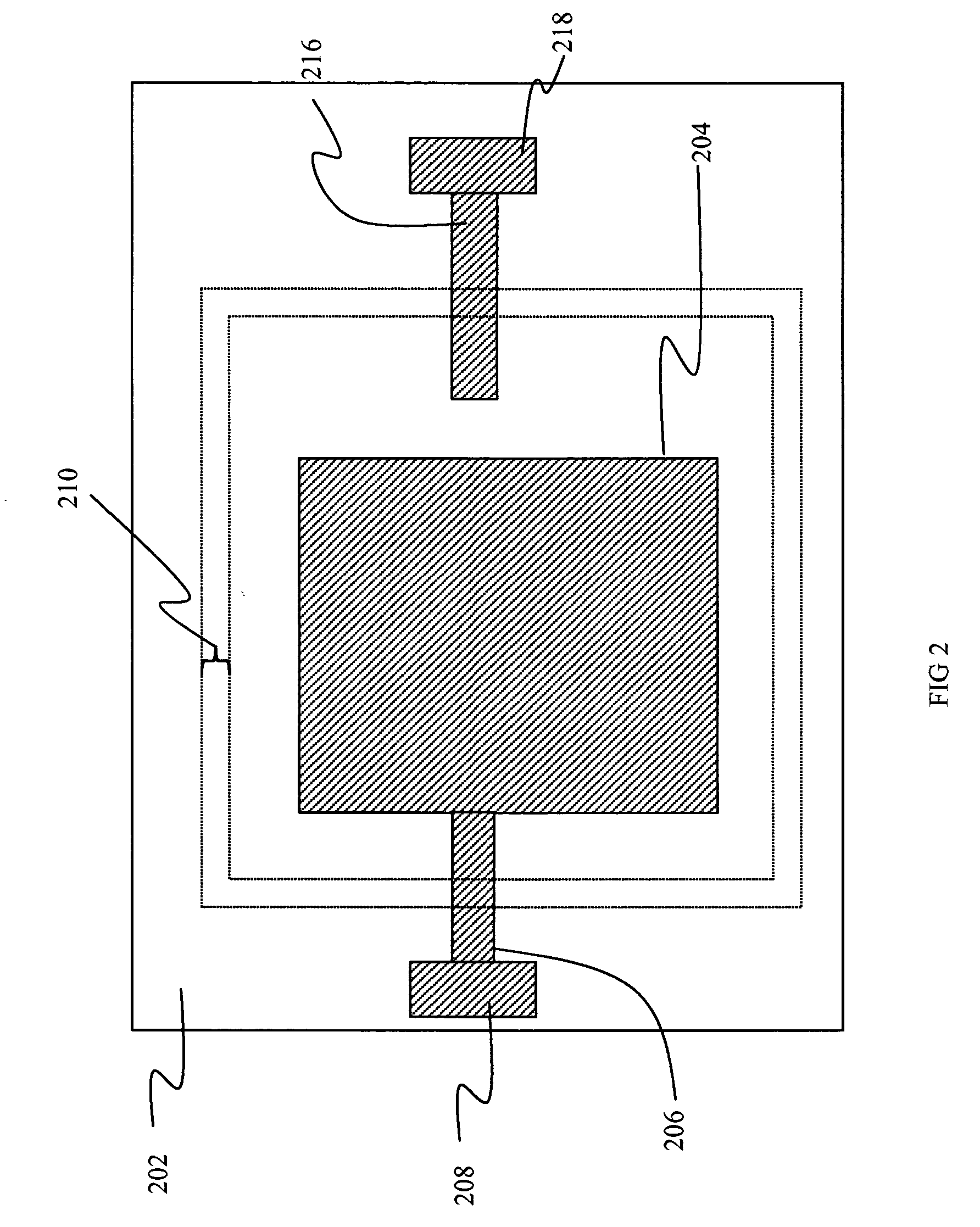
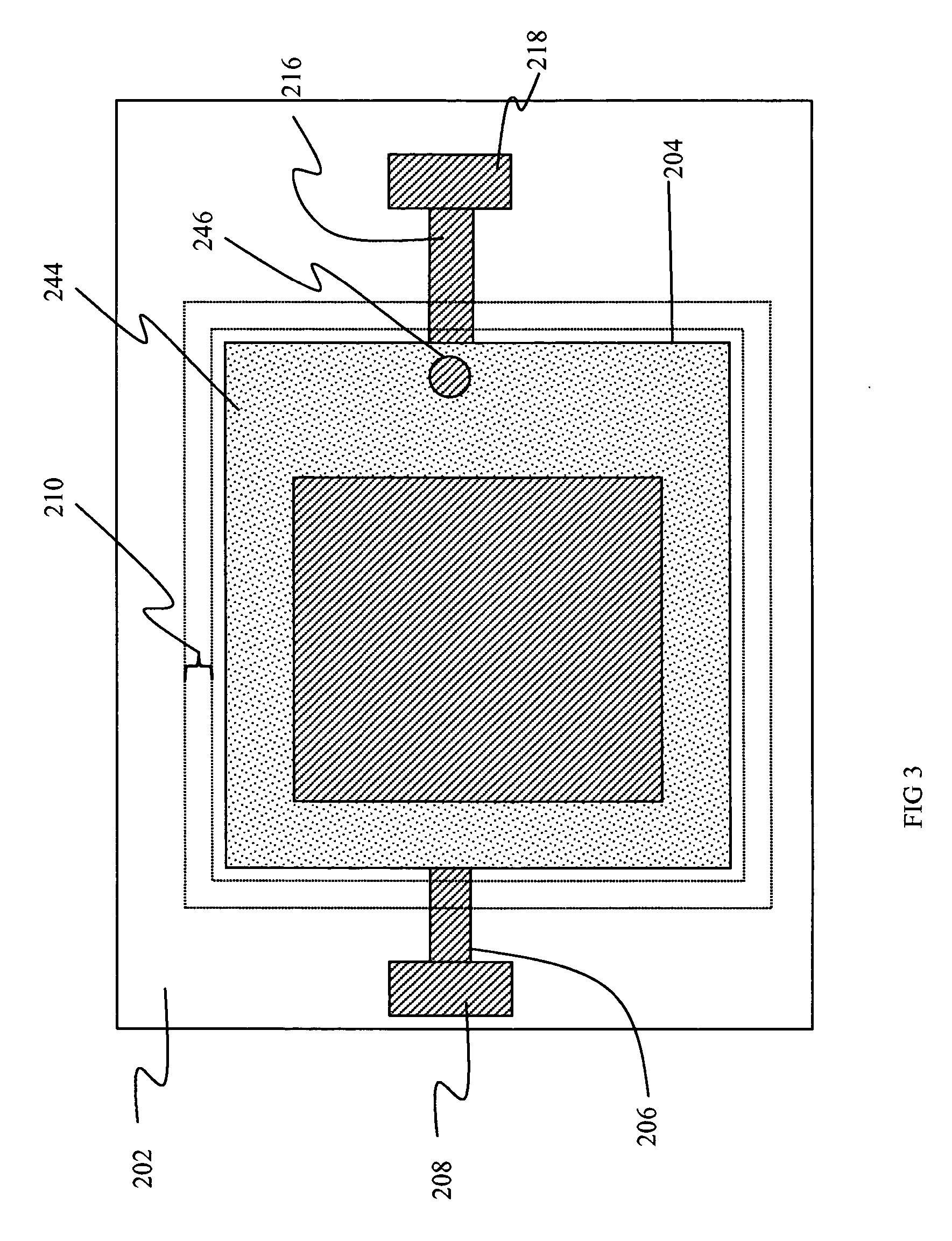
[0151] As a first embodiment, FIGS. 2-4B illustrate various stages of the fabrication of an OLED device 200A. Turning first to FIG. 2, a top view of an OLED substrate 202 is shown. A predetermined seal area 210 is represented by the space between the dotted lines in FIG. 2. The inner dotted line further represents the sealed region of the OLED device. Over OLED substrate 202 are provided a first electrode 204, a first electrical contact pad 208, and a first interconnect line 206 that provides an electrical connection between the first electrode 204 and the first electrical contact pad 208. The first interconnect line 206 extends through the seal area. As discussed later, the first electrode 204 can be the anode or cathode, and can be any number of well known conductive materials, as discussed above. The conductive material used for each of the first electrode 204, the first interconnect line 206, and the first electrical contact pad 208 can be the same or different. In addition, eac...


PUM

PropertyMeasurementUnit
humidityaaaaaaaaaa
transparencyaaaaaaaaaa
temperaturesaaaaaaaaaa

Abstract

A top-emitting OLED device includes a substrate, a first electrode disposed over the substrate, and an organic EL media disposed over the first electrode. The device also includes a transparent or semitransparent second electrode disposed over the organic EL media, and a light transmissive desiccating film having a host and molecularly dispersed desiccant material in such host provided on or over the second electrode.

Description

CROSS REFERENCE TO RELATED APPLICATIONS [0001] Reference is made to commonly assigned U.S. patent application Ser. No. 10 / 946,543 filed Sep. 21, 2004 by Jin-Shan Wang et al., entitled “Lewis Acid Organometallic Desiccant”, U.S. patent application Ser. No. 10 / 946,425 filed Sep. 21, 2004 by Jin-Shan Wang et al., entitled “Desiccant Having a Reactive Salt”, and commonly assigned U.S. patent application Ser. No. ______ filed ______ by Jin-Shan Wang et al., entitled “______”, the disclosures of which are herein incorporated by reference.FIELD OF THE INVENTION [0002] The present invention relates to providing a desiccant for a top-emitting OLED device. BACKGROUND OF THE INVENTION [0003] Various microelectronic devices require restrictions on humidity levels to be in a range of from about 2500 to below 5000 parts per million (ppm) to prevent premature degradation of device performance within a specified operating and / or storage life of the device. Control of the environment to this range o...

Claims


Application Information

Patent Timeline
Patent Type & Authority Applications(United States)
IPC IPC(8): H01L51/52H05B33/02
CPCH01L23/26H01L51/5237H01L2251/5315H01L2924/12044Y10T428/23H01L2924/0002Y10T428/239H01L2924/00H10K50/846H10K2102/3026H10K50/844
Inventor GHOSH, AMALKUMAR P.WANG, JIN-SHANVAZAN, FRIDRICH
Owner EASTMAN KODAK CO
Why Eureka
Try Eureka