

Photomask blank, photomask and fabrication method thereof
- Summary
- Abstract
- Description
- Claims
- Application Information
AI Technical Summary
Benefits of technology
Problems solved by technology
Method used
Image

Examples
example 1
Basic Structure of Photomask Blank
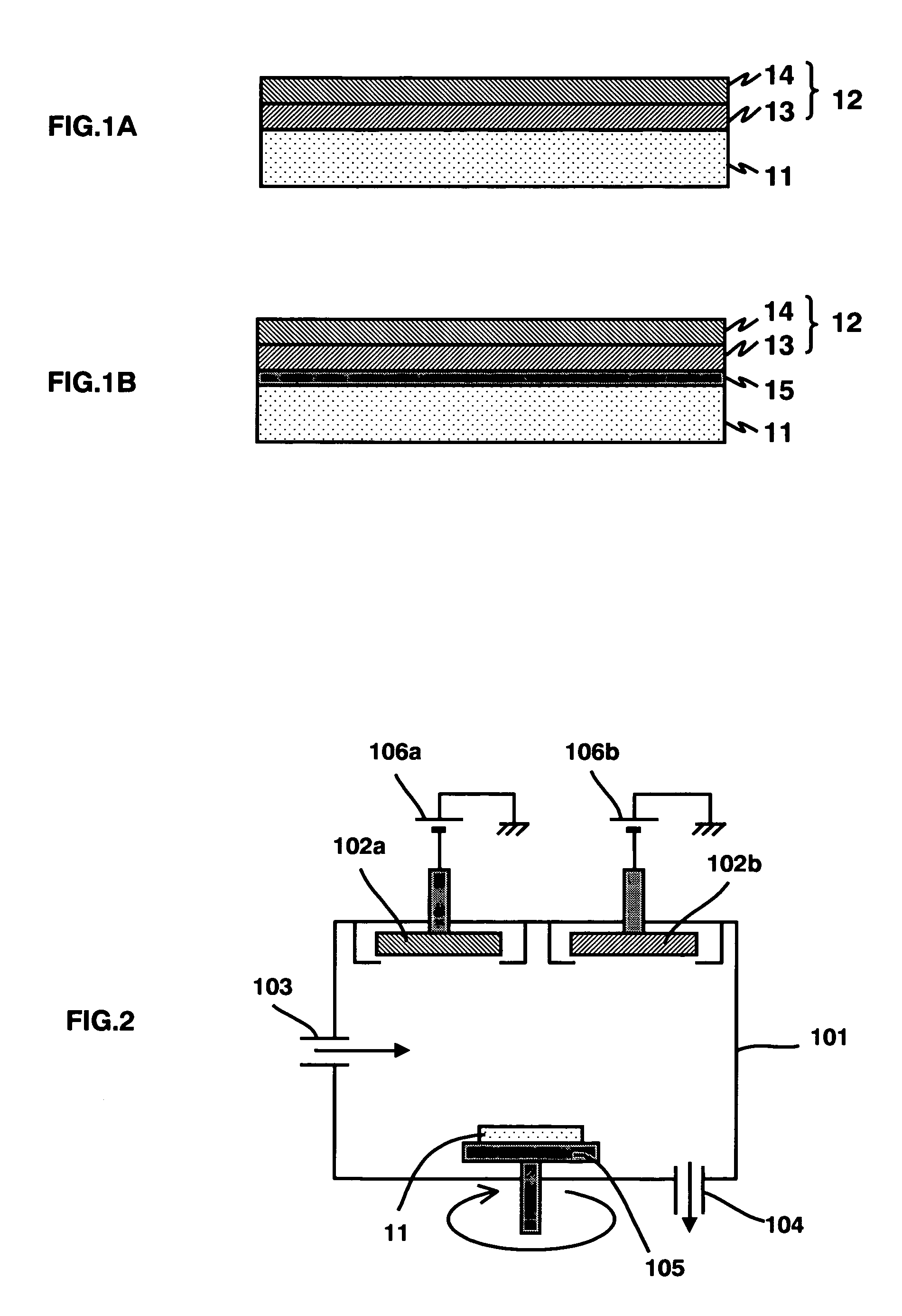
[0054]FIGS. 1A and 1B are schematic cross-sectional views for illustrating a basic structure of a photomask blank according to the present invention. According to this basic structure, as shown in FIG. 1A, the photomask blank comprises an optically transparent substrate 11 and a light-shieldable film 12 formed on one principal plane of the substrate 11, and the light-shieldable film 12 comprises a first light-shieldable film 13 and a second light-shieldable film 14 overlying the first light-shieldable film 13. The substrate 11 may be a typical transparent substrate made of quartz glass, CF2, aluminosilicate glass or the like. The first light-shieldable film 13 is a film that is not substantially etched by fluorine-based dry etching (F-based dry etching) and is primarily composed of chromium. The second light-shieldable film 14 is a film primarily composed of a silicon-containing compound that can be etched by F-based dry etching.
[0055] The silicon...
example 2
Fabrication Process of Photomask Blank
[0073] With regard to this example, there will be described a fabrication process for providing a photomask blank according to the present invention that has the structure described with regard to the example 1.
[0074] [First Light-Shieldable Film (Light-Shielding Film)]
[0075]FIG. 2 is a schematic cross-sectional view for illustrating an arrangement of a sputtering apparatus used for forming the first light-shieldable film of the photomask blank according to the present invention. In this drawing, reference numeral 11 denotes a transparent substrate, which is a 6-inch rectangular quartz substrate, reference numeral 101 denotes a chamber, reference numeral 102a denotes a first target, reference numeral 102b denotes a second target, reference numeral 103 denotes a sputtering gas inlet, reference numeral 104 denotes a gas outlet, reference numeral 105 denotes a substrate rotating table, and reference numerals 106a and 106b denote power supplies th...
example 3
Fabrication Process of Binary Photomask
[0102] With regard to this example, a fabrication process for providing a photomask using a photomask blank according to the present invention will be described. In the following description, it will be supposed that the photomask is a binary mask.
[0103]FIGS. 5A to 5E are diagrams for illustrating a fabrication process of a binary photomask. First, a photoresist film 16 is applied onto a light-shieldable film 12 on a substrate 11 (FIG. 5A), and the photoresist 16 is patterned to form a resist pattern 17 for circuit pattern writing (FIG. 5B). Preferably, before applying the photoresist film 16, the substrate is surface-treated to reduce the surface energy thereof. This treatment is intended to prevent the resist mask having been finely patterned from peeling off or falling during a subsequent step.
[0104] The most preferable surface treatment is a process of alkylsilycating the surface of the substrate (actually, the surface of the light-shiel...
PUM
| Property | Measurement | Unit |
|---|---|---|
| Thickness | aaaaa | aaaaa |
| Thickness | aaaaa | aaaaa |
| Thickness | aaaaa | aaaaa |
Abstract
Description
Claims
Application Information