Methods of fabricating a semiconductor device using a selective epitaxial growth technique
- Summary
- Abstract
- Description
- Claims
- Application Information
AI Technical Summary
Benefits of technology
Problems solved by technology
Method used
Image


Examples
Embodiment Construction
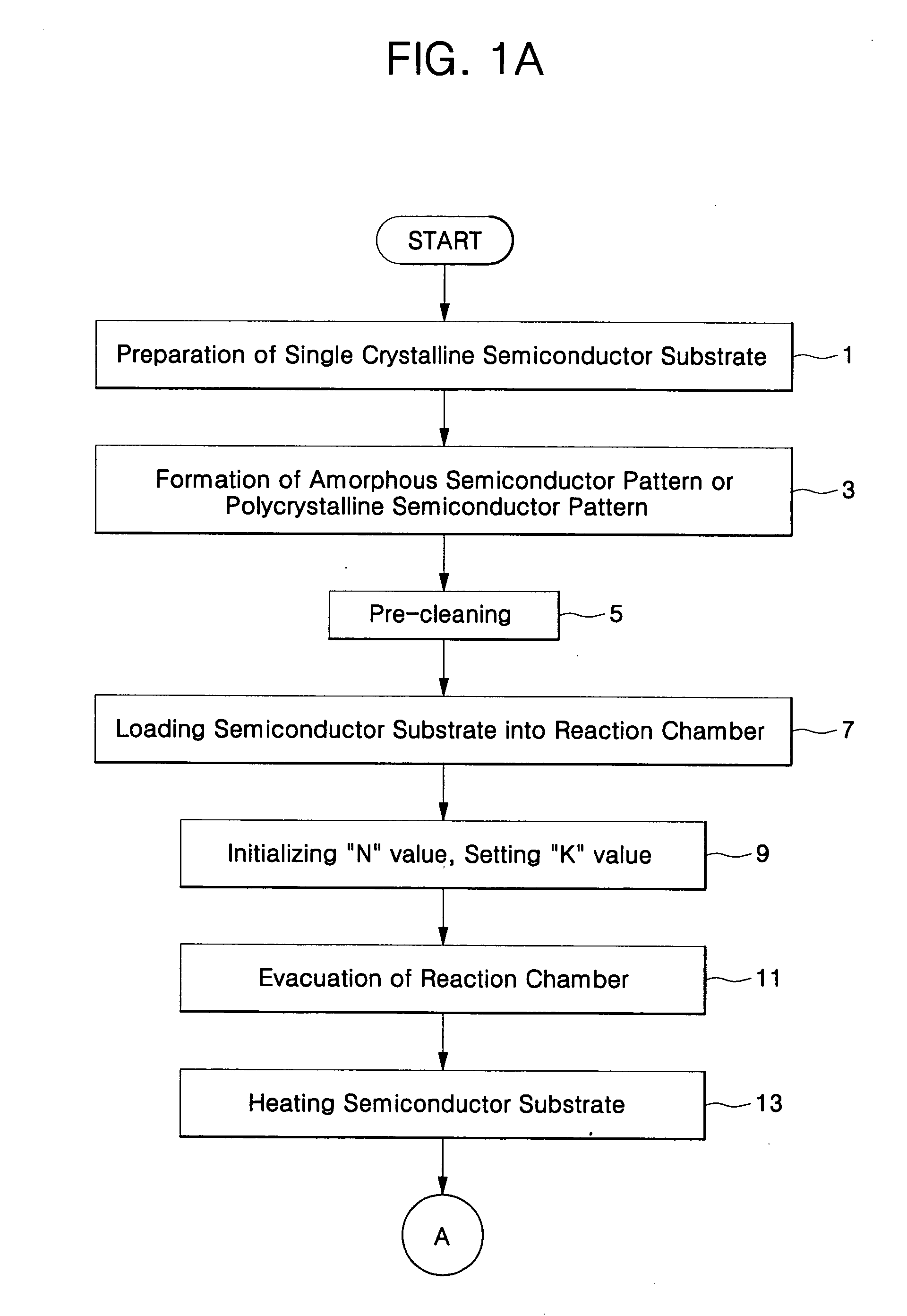
[0052] The present invention will now be described more fully hereinafter with reference to the accompanying drawings, in which preferred embodiments of the invention are shown. This invention may, however, be embodied in different forms and should not be construed as limited to the embodiments set forth herein. In the drawings, the thickness of layers and regions are exaggerated for clarity. Like numbers refer to like elements throughout the specification.
[0053]FIGS. 1A and 1B are process flow charts illustrating a selective epitaxial growth process in accordance with embodiments of the present invention, and FIGS. 2 to 5 are cross-sectional views illustrating methods of fabricating MOS transistors using the selective epitaxial growth technique in accordance with embodiment of the present invention.
[0054] Referring to FIGS. 1A, 1B and 2, a single crystalline semiconductor substrate 51 is prepared (step 1 of FIG. 1A). The single crystalline semiconductor substrate 51 can be, for e...
PUM
 Abstract
Description
Claims
Application Information
 - R&D
- Intellectual Property
- Life Sciences
- Materials
- Tech Scout
- Unparalleled Data Quality
- Higher Quality Content
- 60% Fewer Hallucinations
Browse by: Latest US Patents, China's latest patents, Technical Efficacy Thesaurus, Application Domain, Technology Topic, Popular Technical Reports.
© 2025 PatSnap. All rights reserved.Legal|Privacy policy|Modern Slavery Act Transparency Statement|Sitemap|About US| Contact US: help@patsnap.com