Memory device verification of multiple write operations

a memory device and write operation technology, applied in memory systems, error detection/correction, instruments, etc., can solve the problems of large number of system crashes affecting users, high cost, and only available characteristics on complex, high-performance data processing systems. , to achieve the effect of substantially reducing the processing and communication bandwidth consumed by the process

Inactive Publication Date: 2006-04-27
IBM CORP
View PDF9 Cites 65 Cited by
  • Summary
  • Abstract
  • Description
  • Claims
  • Application Information

AI Technical Summary

Benefits of technology

[0011] The invention addresses these and other problems associated with the prior art by utilizing individual verification operations that are effectively capable of verifying multiple associated write operations. In particular, a verification operation consistent with the invention may be initiated after the issuance of a plurality of write operations that initiate the storage of data to a memory s

Problems solved by technology

Data integrity is of particular concern, for example, in fault tolerant applications such as servers, databases, scientific computers, and the like, where any errors whatsoever could jeopardize the accuracy of complex operations and/or cause system crashes that affect large numbers of users.
Data integrity issues are a concern, for example, for many solid state memory arrays such as those used as the main working storage repository for a data processing system.
A significant amount of effort has been directed toward detecting and correcting errors in memory devices during power up of a data processing system, as well as during the normal operation of such a system.
Often such characteristics are expensive and only available on complex, high performance data processing systems.
Furthermore, in many instances, many types of errors go beyond the ability of a conventional system to do anything other than “crash” and require a physical repair before normal device operation can be restored.
Despite the advances made in terms of error detection and correc

Method used


Image

  • Memory device verification of multiple write operations
  • Memory device verification of multiple write operations
  • Memory device verification of multiple write operations

Examples


Embodiment Construction

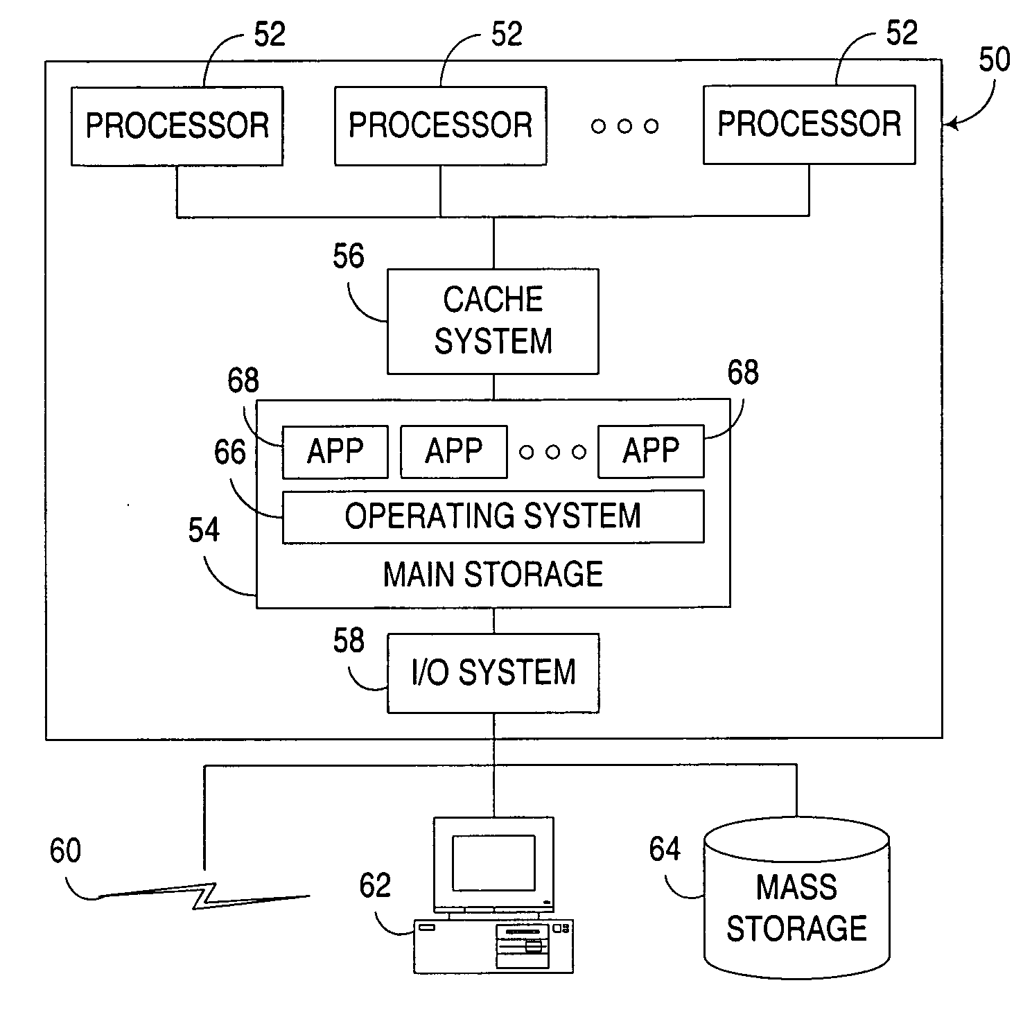
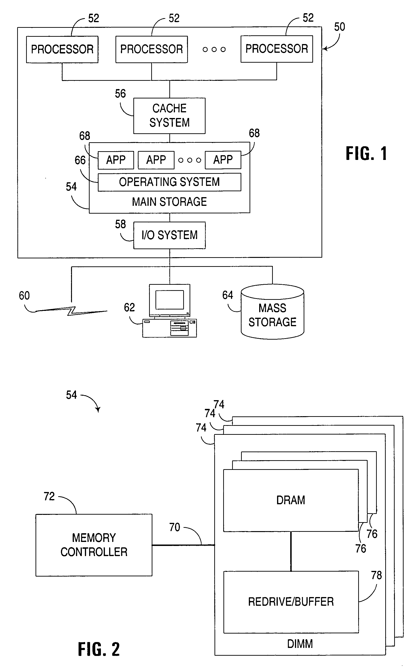
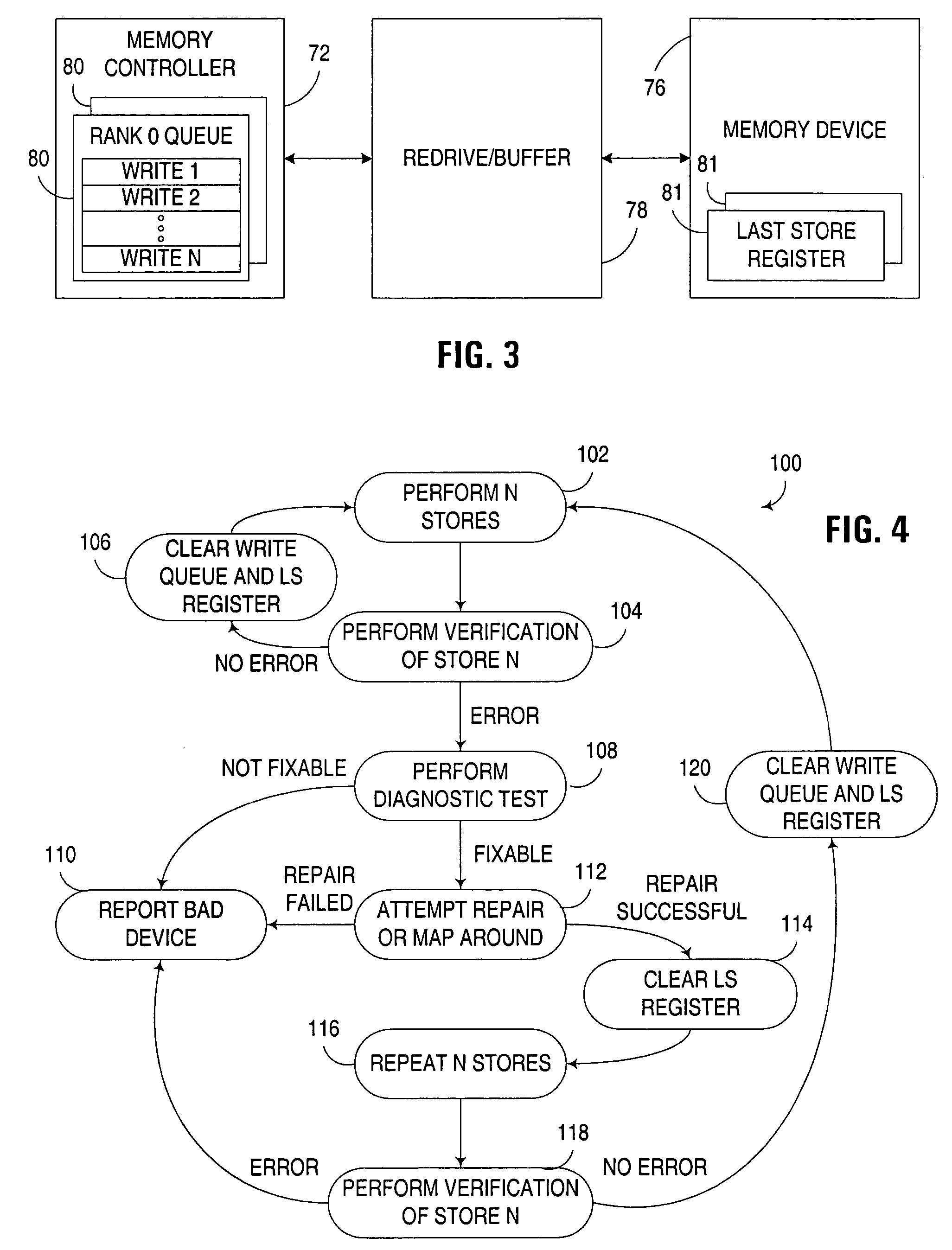
[0024] The embodiments discussed and illustrated hereinafter utilize verification operations that are configured to verify only a subset of data written to a memory storage device by a plurality of preceding write operations, thus reducing the overhead associated with write verification that would otherwise be required were each write operation individually verified. In this context, a write operation may alternatively be referred to as a store operation, or simply a “write” or “store”.

[0025] In many embodiments consistent with the invention, verification−operations are configured to operate on a basic principle of verifying a fraction or subset of the data that gets written to a memory device, a collection of memory devices, a memory array, or other subset of a physical memory space, but queue up all of the data written thereto between these more infrequent verification operations. As will become more apparent below, write verification may be performed at different levels of a mem...


PUM


Abstract

Verification operations are utilized to effectively verify multiple associated write operations. A verification operation may be initiated after the issuance of a plurality of write operations that initiate the storage of data to a memory storage device, and may be configured to verify only a subset of the data written to the memory storage device by the plurality of write operations. As a result, verification operations are not required to be performed after each write operation, and consequently, the number of verification operations, and thus the processing and communication bandwidth consumed thereby, can be substantially reduced.

Description

FIELD OF THE INVENTION [0001] The invention relates to computers and data processing systems, and in particular to performing verifying write operations processed by memory devices utilized in such computers and data processing systems. BACKGROUND OF THE INVENTION [0002] Ensuring the integrity of data processed by a data processing system such as a computer or like electronic device is critical for the reliable operation of such a system. Data integrity is of particular concern, for example, in fault tolerant applications such as servers, databases, scientific computers, and the like, where any errors whatsoever could jeopardize the accuracy of complex operations and / or cause system crashes that affect large numbers of users. [0003] Data integrity issues are a concern, for example, for many solid state memory arrays such as those used as the main working storage repository for a data processing system. Solid state memory arrays are typically implemented using multiple integrated cir...

Claims


Application Information

Patent Timeline
IPC IPC(8): G01R31/28G06F11/00
CPCG06F12/0804G06F12/084
Inventor COCHRAN, WILLIAM HUGHHOVIS, WILLIAM PAULRUDRUD, PAUL
Owner IBM CORP
Why Eureka
Try Eureka