Active matrix type organic light emitting diode device and fabrication method thereof

a light-emitting diode and active matrix technology, which is applied in the direction of solid-state devices, electric lighting sources, electric light sources, etc., can solve the problems of more severe moiré problems, interference phenomena of light, and lcd devices having moiré problems, so as to enhance the characteristics of the screen

Active Publication Date: 2006-05-04
LG DISPLAY CO LTD
View PDF1 Cites 78 Cited by
  • Summary
  • Abstract
  • Description
  • Claims
  • Application Information

AI Technical Summary

Benefits of technology

[0041] Another object of the present invention is to provide an active matrix type organic light emitting diode (AMOLED) device capable of enhancing characteristics of a screen by removing a moiré phenomenon when the AMOLED device is crystallized, and its fabrication method.

Problems solved by technology

However, since the LCD device is a passive device, not a self-light emitting device, and because of its technical limitations with respect to brightness, contrast, a viewing angle and enlargement of screen, there have been efforts to develop a new flat panel display that can overcome such shortcomings of the LCD device.
In this case, as shown in FIG. 3, moiré in the pattern of a comb-teeth is generated, which is a problem.
A major cause of the moiré phenomenon is an interference phenomenon of light.
The moiré phenomenon must be solved with respect to an image display device such as the liquid crystal display (LCD) device, and is quite problematic in case of an EL image display device using the EL as a light emitting device.
Both the EL image display device and the LCD device do have the moiré problem.
However, the moiré problem is more severe in the EL that does not have a polarization plate as in the LCD device.

Method used


Image

  • Active matrix type organic light emitting diode device and fabrication method thereof
  • Active matrix type organic light emitting diode device and fabrication method thereof
  • Active matrix type organic light emitting diode device and fabrication method thereof

Examples


Embodiment Construction

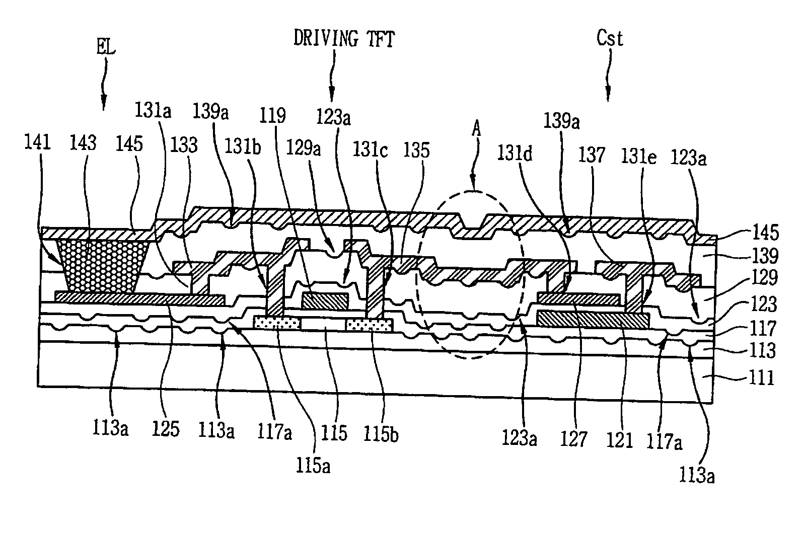
[0057]FIG. 4 is a sectional view of an AMOLED device in accordance with the present invention, FIG. 5 is an enlarged view of the portion ‘A’ in FIG. 4, showing a stacked state of insulation films with a plurality of recesses formed therein, and FIG. 6 is a plan view showing an example of a plurality of irregularly-patterned recesses formed on a surface of an insulation film during a fabrication process of the AMOLED device. Although FIG. 4 focuses on a unit pixel including a switch TFT, a storage capacitor Cst, a driving TFT and an EL, all operatively coupled, the AMOLED device has a plurality of such unit pixels in a known matrix arrangement.

[0058] As shown in FIGS. 4 and 5, the AMOLED device in accordance with the present invention is constructed such that a buffer layer 113 with a plurality of first recesses 113a formed thereon is formed on an insulation substrate 110 and a semiconductor layer 115 made of polysilicon with a drain electrode region 115b and a source electrode regi...


PUM


Abstract

An active matrix type organic light emitting diode (AMOLED) device and its fabrication method are discussed. In one embodiment, an OLED device includes an EL configured to emit light, a driving TFT configured to control the EL, a storage capacitor coupled to the driving TFT, and at least one insulation layer configured to insulate at least one of the EL, the driving TFT and the storage capacitor, and including a plurality of recesses formed on a surface of the at least one insulation layer.

Description

[0001] This Nonprovisional application claims priority under 35 U.S.C. § 119 on Patent Application No. 10-2004-0087479 filed in the Republic of Korea on Oct. 29, 2004, the entire contents of which are hereby incorporated by reference. BACKGROUND OF THE INVENTION [0002] 1. Field of the Invention [0003] The present invention relates to an active matrix type organic light emitting diode (AMOLED) device and, more particularly, to an AMOLED device using a polysilicon thin film transistor (TFT) capable of removing a moire phenomenon and its fabrication method. [0004] 2. Description of the Related Art [0005] Recently, a liquid crystal display (LCD) device is widely preferred to be used as a flat panel display due to its light weight and low power consumption. However, since the LCD device is a passive device, not a self-light emitting device, and because of its technical limitations with respect to brightness, contrast, a viewing angle and enlargement of screen, there have been efforts to ...

Claims


Application Information

Patent Timeline
Patent Type & Authority Applications(United States)
IPC IPC(8): H01L29/04
CPCH01L27/12H01L27/1248H01L51/5281H01L27/3244H10K59/124H10K59/12H10K50/86H10K59/1201H05B33/00H05B33/10H05B33/22
Inventor LEE, KYUNG-EON
Owner LG DISPLAY CO LTD
Why Eureka
Try Eureka