Hybrid type integrated optical device

a technology of integrated optical devices and hybrid optics, which is applied in the direction of optical elements, instruments, semiconductor lasers, etc., can solve the problems of raising the price of semiconductors, and achieve the effect of reducing the size of the air gap and enhance the optical coupling efficiency

Inactive Publication Date: 2006-05-04
ELECTRONICS & TELECOMM RES INST
View PDF10 Cites 67 Cited by
  • Summary
  • Abstract
  • Description
  • Claims
  • Application Information

AI Technical Summary

Benefits of technology

[0016] The present invention has been made to solve the above problems, and it is an object of the present invention to provide a hybrid type integrated optical device, designed to enhance optical coupling efficiency by reproducibly reducing a size of an air gap between a semiconductor laser and a planar waveguide platform.

Problems solved by technology

As such, accuracy required for the process of manufacturing the optical mode size converter causes a problem of raising the price of the semiconductor together with the price of the hybrid type integrated optical device manufactured by use of the semiconductor laser.

Method used


Image

  • Hybrid type integrated optical device
  • Hybrid type integrated optical device
  • Hybrid type integrated optical device

Examples


Embodiment Construction

[0034] Preferred embodiments will now be described in detail with reference to the accompanying drawings.

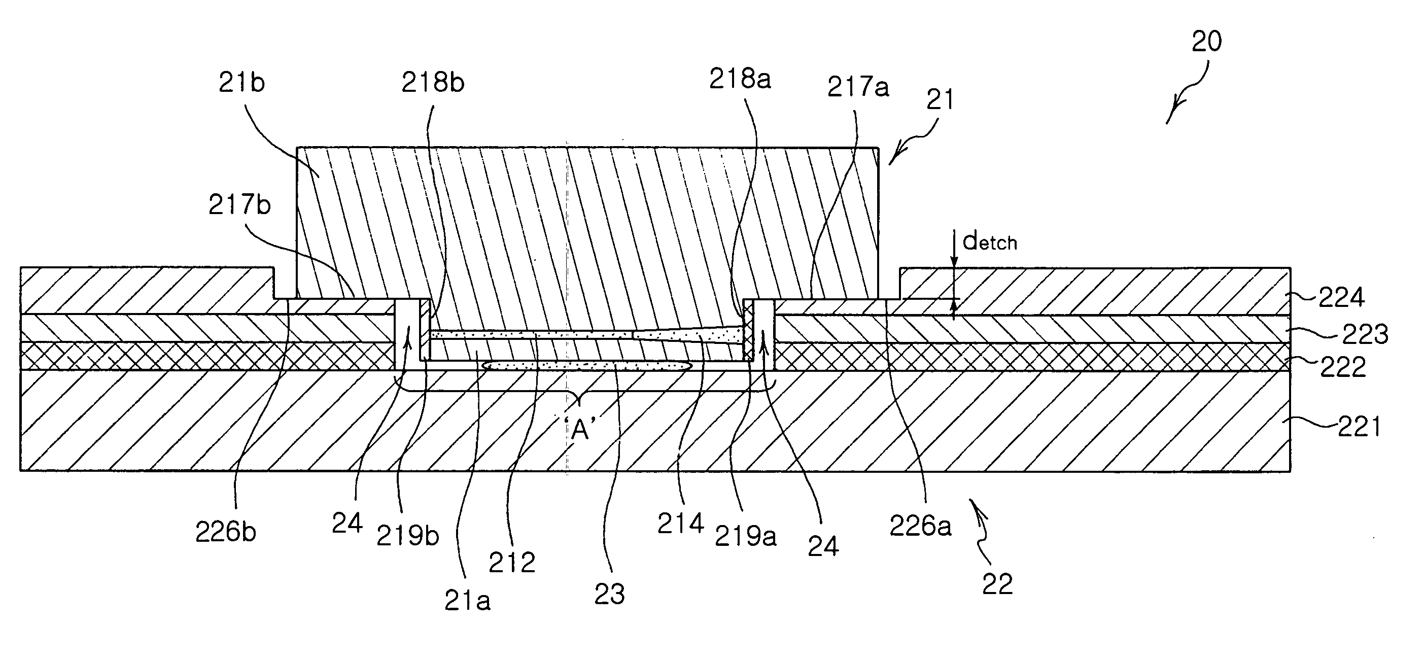
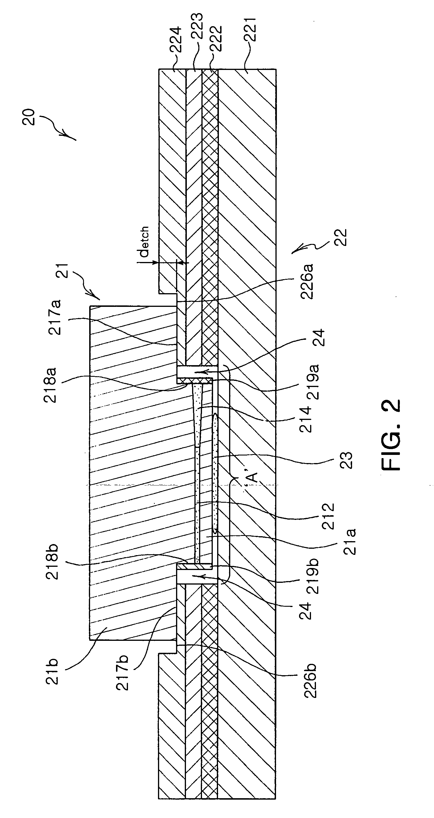
[0035]FIG. 2 is a cross-sectional view illustrating a hybrid type integrated optical device according to one embodiment of the present invention. Referring to FIG. 2, the hybrid type integrated optical device according to the present embodiment comprises: a semiconductor laser 21 including a first structure 21a, which has an active region 212 and a light emission surface 218a formed on at least one side surface of the first structure 21a, and a second structure 21b, which is formed below the first structure 21a and has upper surfaces 217a and 217b respectively exposed at the light emission surface 218a and the other side surface opposite to the light emitting surface 218a; and a planar waveguide platform 22 including a substrate 221, a lower clad layer 222, a core layer 223, an upper clad layer 224, sequentially stacked in this order on the substrate 221 such that a predetermine...


PUM


Abstract

A hybrid type integrated optical device has a semiconductor laser mounted on a planar waveguide platform by flip-chip bonding. The optical device comprises a semiconductor laser and a planar waveguide platform. The semiconductor laser includes a first structure, which has an active region and a light emission surface formed on at least one side surface of the first structure, and a second structure, which is formed below the first structure and has upper surfaces exposed at the light emission surface of the first structure and/or to a surface opposite to the light emitting surface. The planar waveguide platform includes a substrate, a lower clad layer, a core layer, and an upper clad layer, being sequentially stacked on the substrate. The semiconductor laser is flip-chip bonded on the substrate, such that the exposed upper surfaces of the second structure contact the upper surface of the upper clad layer.

Description

RELATED APPLICATIONS [0001] The present application is based on, and claims priority from, Korean Application Number 2004-89059, filed Nov. 3, 2004, the disclosure of which is incorporated by reference herein in the entirety. BACKGROUND OF THE INVENTION [0002] 1. Field of the Invention [0003] The present invention relates to a hybrid type integrated optical device, which has a semiconductor laser mounted on a planar waveguide platform by flip-chip bonding, and more particularly to a hybrid type integrated optical device, designed to allow effective vertical alignment of an optical axis of a semiconductor laser and to reproducibly reduce an air gap between a planar waveguide platform and the semiconductor laser so as to provide high optical coupling efficiency between the planar waveguide platform and the semiconductor laser. [0004] 2. Description of the Related Art [0005] Hybrid type integrated optical devices are generally manufactured by coupling a semiconductor laser and a planar...

Claims


Application Information

Patent Timeline
Patent Type & Authority Applications(United States)
IPC IPC(8): H01S5/00H01S3/08G02B6/12
CPCG02B6/4207G02B6/4232G02B2006/12121H01S5/0224H01S5/02252H01S5/0226H01S5/1014H01S5/227H01S2301/176H01S5/02326H01S5/0234H01S5/0236G02B2006/12128
Inventor PARK, MAHN YONGKIM, BYOUNG WHI
Owner ELECTRONICS & TELECOMM RES INST
Why Eureka
Try Eureka