

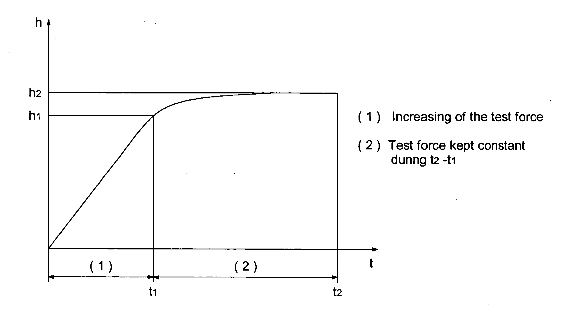
Organic photoconductor, image forming method, image forming apparatus and process cartridge
a photoconductor and organic technology, applied in the direction of electrographic process, corona discharge, instruments, etc., can solve the problems of poor mechanical strength, susceptibility to deterioration or damage on the surface of the photoconductor, and inability to form toner films on the photoconductor, so as to facilitate the removal of remaining toner, improve the toner transfer properties, and improve the effect of sharpness
- Summary
- Abstract
- Description
- Claims
- Application Information
AI Technical Summary
Benefits of technology
Problems solved by technology
Method used
Image

Examples
examples
[0126] Referring to embodiments, the following describes the details of the present invention, without the present invention being restricted thereto. The parts in the following description refer to “parts by mass”.
[0127] Production of Photoconductor 1
[0128] A photoconductor 1 was produced as described below:
[0129] The surface of a 100 mm-diameter, 346 mm long cylindrical aluminum support member was machined to get a conductive support having a surface roughness of Rz=1.5 (μm).
[0130]
[0131] The following dispersion solution of the intermediate layer was diluted twofold with the same mixed solvent, and it was left to stand overnight. Then it was filtered by a filter (a 5-μm filter, Rigimesh by Nihon Pall Ltd.) to prepare the intermediate layer coating solution.
[0132] 1 part of Polyamide resin CM 8000 (by Toray Industries, Inc.)
[0133] 3 parts of titanium oxide SMT500SAS (by Teika Inc.)
[0134] 10 parts of methanol
[0135] A sand mill was used as a dispersion machine to perform disp...
PUM
| Property | Measurement | Unit |
|---|---|---|
| Length | aaaaa | aaaaa |
| Length | aaaaa | aaaaa |
| Fraction | aaaaa | aaaaa |
Abstract
Description
Claims
Application Information