Method of verifying electron beam data

a technology of electron beam data and electron beam data, which is applied in the field of electron beam data verification, can solve the problems of deformation of distorted electron beam data, and deformation of certain regions of design data,

Inactive Publication Date: 2006-05-04
SAMSUNG ELECTRONICS CO LTD
View PDF12 Cites 0 Cited by
  • Summary
  • Abstract
  • Description
  • Claims
  • Application Information

AI Technical Summary

Problems solved by technology

Unfortunately, the electron beam data produced by the conversion process may have some problems that could lead to defects in the photomask, and therefore defects in a semiconductor device formed with the photomask.
For example, certain regions of the design data may be missing, distorted, or otherwise poorly formed in the electron beam data.
Because the patterns represented by the design data and the electron beam data are generally extensive and intricate, and because the geometric design requirements for each of the smaller patterns are typically interdependent, a large amount of computation may be required to perform the verification process.
In addition to the problems described above, existing methods of performing the conversion and verification processes may experience further problems where the size of the design data increases and an optical proximity effect correction is applied to the electron beam data.
Accordingly, it takes a long time and requires significant system resources for data converting device 20 to convert the design data into the electron beam data.
Also, errors with unidentified causes may appear in the electron beam data as the design data becomes larger and larger.
Otherwise, an error signal is generated (230), causing the conversion process to terminate.
As described above, it takes long time and requires significant computing resources to convert the design data into the converted electron beam data.
Unfortunately, the conventional methods described in relation to FIGS. 2 and 3 require the conversion to take place twice.
Performing the conversion twice is inefficient.

Method used


Image

  • Method of verifying electron beam data
  • Method of verifying electron beam data
  • Method of verifying electron beam data

Examples


Embodiment Construction

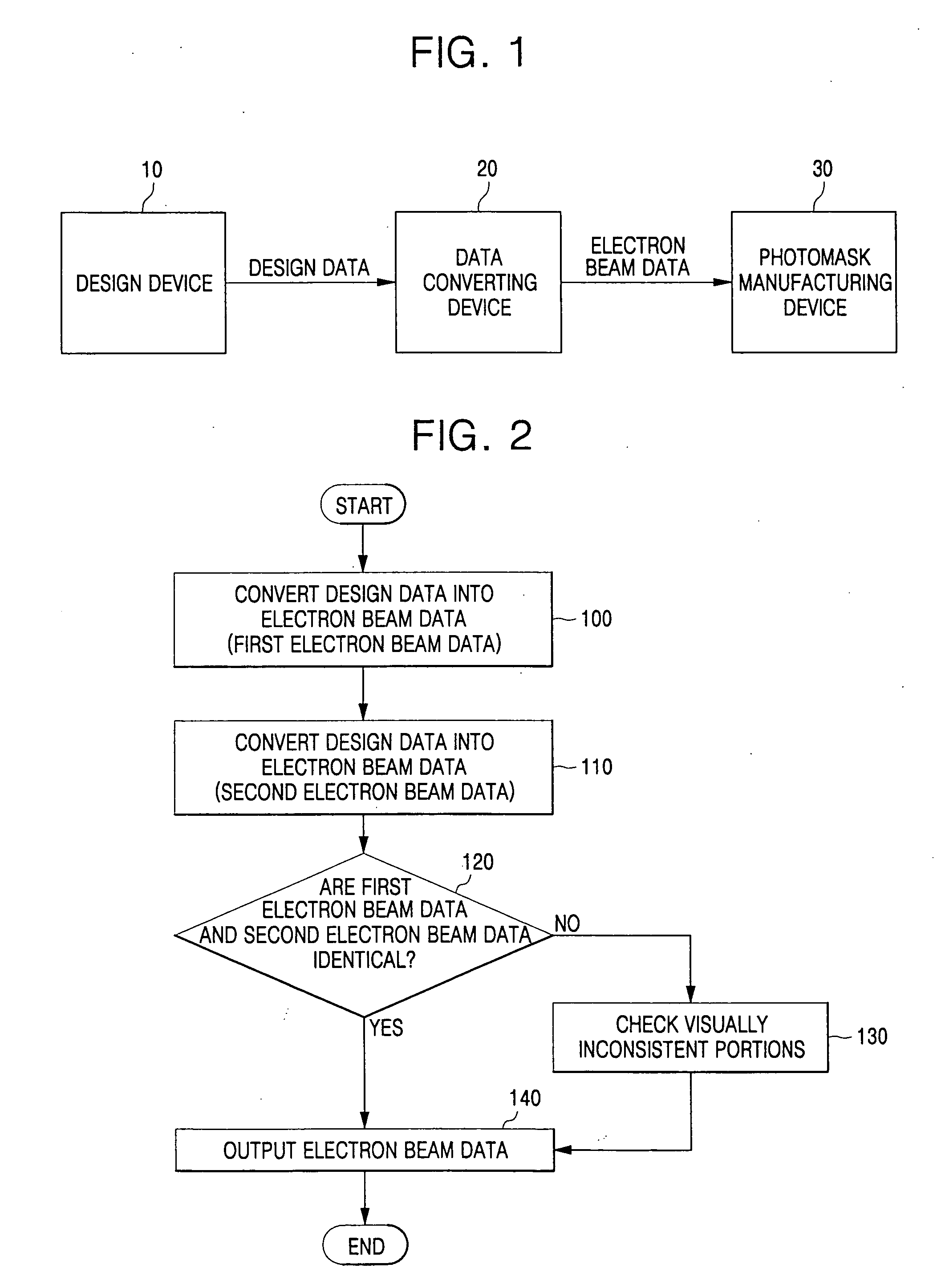
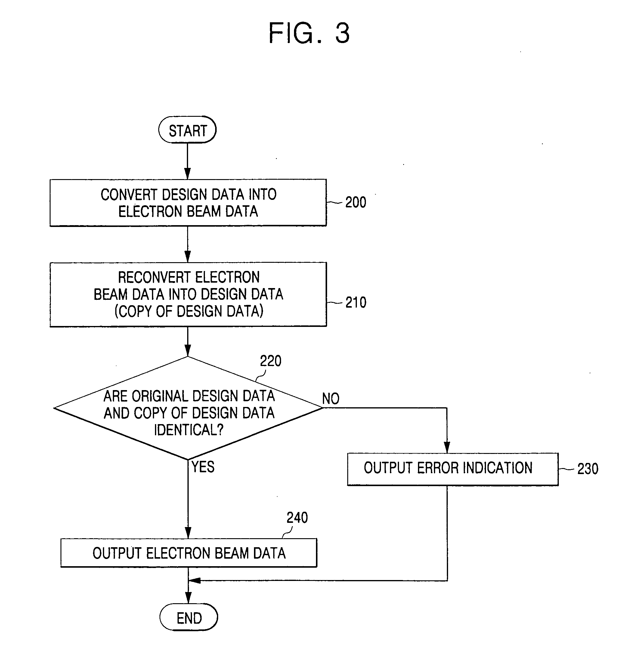
[0035] Exemplary embodiments of the invention are described below with reference to the corresponding drawings. These embodiments are presented as teaching examples. The actual scope of the invention is defined by the claims that follow.

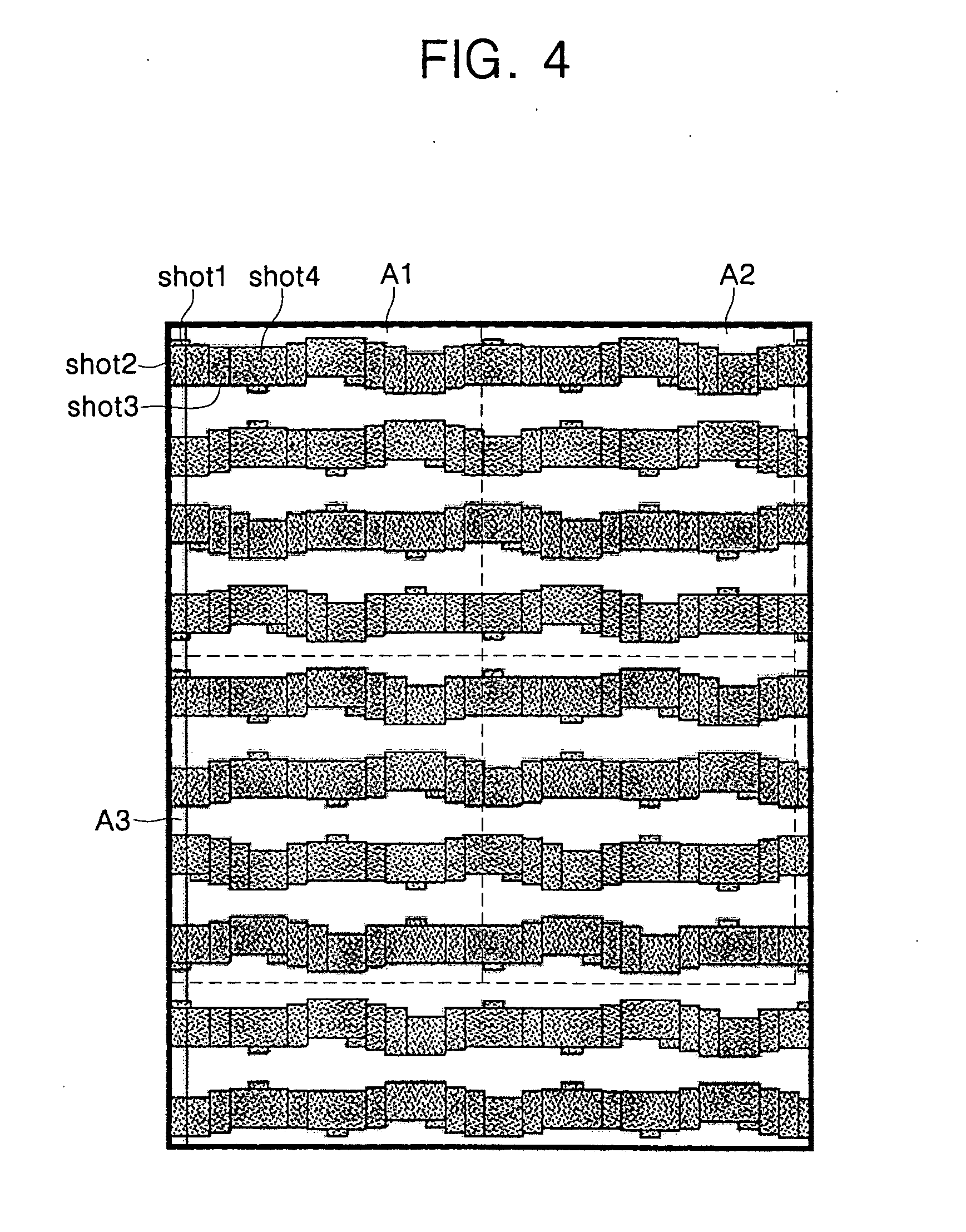
[0036]FIG. 4 is a diagram of electron beam data defining a pattern to be formed on a photomask. In FIG. 4, the electron beam data comprises a plurality of polygons (rectangles), each corresponding to a “shot” of an electron beam that will be applied to a blank photomask to form the pattern. The polygons are labeled in FIG. 4 as “shot1”, “shot2”, etc.

[0037] As seen in FIG. 4, the pattern comprises multiple repetitive regions, labeled A1 through A3 and delineated by broken lines. Repetitive regions frequently occur in electron beam data used to form photomasks for semiconductor devices characterized by repetitive elements. For example, a memory cell array of a semiconductor memory device typically comprises a plurality of memory cells arranged in a r...


PUM

PropertyMeasurementUnit
areaaaaaaaaaaa
sizesaaaaaaaaaa
electron beamaaaaaaaaaa

Abstract

A method of verifying electron beam data used to produce a photomask comprises dividing design data for the photomask into a plurality of repetitive regions, sequentially converting the sequential regions into electron beam data, and determining whether electron beam data corresponding to a current repetitive region is substantially identical to electron beam data corresponding to a previous repetitive region.

Description

BACKGROUND OF THE INVENTION [0001] 1. Field of the Invention [0002] The present invention relates generally to a method of verifying electron beam data used to form a photomask for a semiconductor manufacturing device. More particularly, the invention relates to a method of verifying the electron beam data by comparing electron beam data produced for one region of the photomask with electron beam data produced for another area region of the photomask. [0003] This application claims the benefit of Korean Patent Application No. 2004-0088510, filed Nov. 2, 2004, the disclosure of which is hereby incorporated by reference in its entirety. [0004] 2. Description of the Related Art [0005] Photolithography is a common process used in the manufacture of semiconductor devices such as computer processor chips, memory and the like. In general, photolithography is used to form conductive patterns in a semiconductor substrate. The conductive patterns are typically formed by creating a layer of re...

Claims


Application Information

Patent Timeline
Patent Type & Authority Applications(United States)
IPC IPC(8): G03C5/00G03F1/20G03F1/78G03F1/86
CPCH01J37/3026H01J2237/31762G03F1/68G03F7/2051G03F7/70383H01J37/3174
Inventor JANG, SUNG-HOONAHN, BYOUNG-SUPNO, YOUNG-HWA
Owner SAMSUNG ELECTRONICS CO LTD
Why Eureka
Try Eureka