Method for fabricating semiconductor components

a semiconductor and component technology, applied in semiconductor devices, semiconductor/solid-state device details, electrical devices, etc., can solve the disadvantage of multiple method steps for fabricating external contact connections, inability to carry out method steps in parallel for a plurality of semiconductor components, and too small dimensions. problem, to achieve the effect of reducing the number of method steps

Inactive Publication Date: 2006-05-04
INFINEON TECH AG
View PDF3 Cites 59 Cited by
  • Summary
  • Abstract
  • Description
  • Claims
  • Application Information

AI Technical Summary

Benefits of technology

[0007] It is an object of the present invention to provide an improved method which manages with a smaller numb

Problems solved by technology

However, these semiconductor contact-connection regions have dimensions which are too small for these semiconductor contact-connection regions to be directly contact-connected using method techniques associated with final assembly of semiconductor components.
A multiplicity of individual method steps for fabricating the external contact-connection are disadvantageously required for these semiconductor tec

Method used


Image

  • Method for fabricating semiconductor components
  • Method for fabricating semiconductor components
  • Method for fabricating semiconductor components

Examples


first embodiment

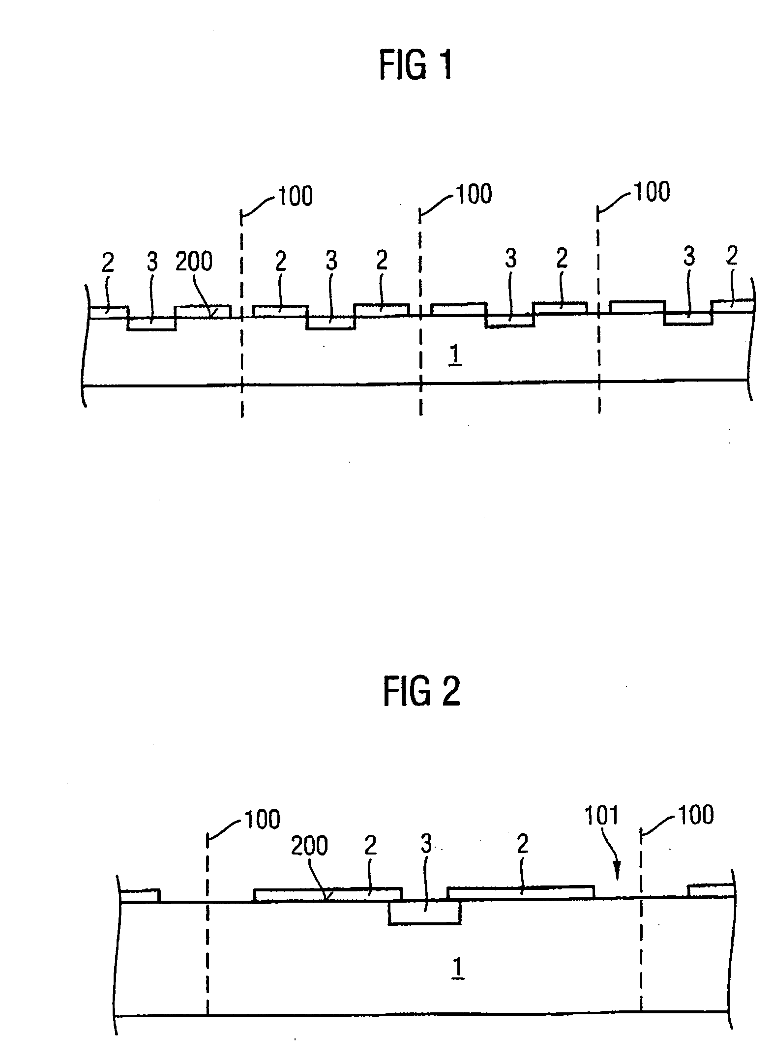
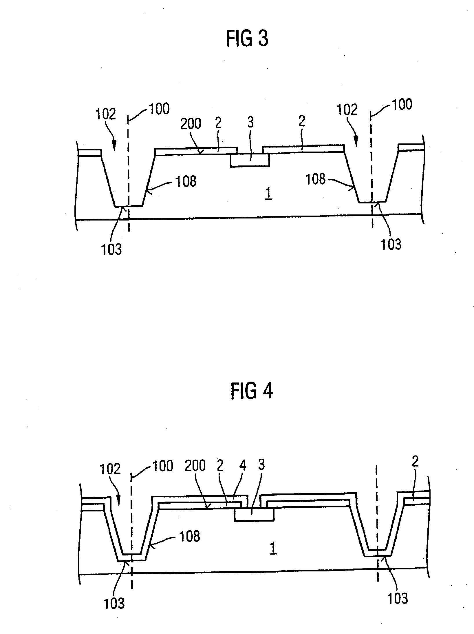
[0028]FIG. 2 illustrates a partial section for illustrating the present invention. A detail from FIG. 1 having a single semiconductor component is illustrated in this case. A sawing track 101 is introduced along the boundary line 100. This sawing track 101 borders the semiconductor component. In a first method step, a conically shaped saw blade is used to saw a trench 102 into the substrate 1 along the sawing track 101 or the boundary lines 100. The conical saw blade results in a trench bottom 103 whose dimensions are smaller than the opening of the trench at the surface 200. In addition, the sidewalls 108 of the trench are inclined (FIG. 3). In a subsequent method step, a nonconductive insulation layer 4 is applied to the wafer (FIG. 4). The nonconductive insulation layer 4 covers both the trench 102 and the entire surface 200 and the semiconductor contact-connection region 3. A patterning process is used to remove the insulation layer 4 at least partially from the semiconductor co...

third embodiment

[0031]FIG. 11 illustrates another embodiment of the present invention, the semiconductor component being potted using a potting compound 14 after it has been mounted on a carrier 10 (reconstituted wafer). The potting compound 14 advantageously protects the component from mechanical loads. FIG. 12 illustrates a semiconductor component which was fabricated in accordance with the present invention. To this end, the front end wafer was sawn in a first method step in order to singulate the semiconductor components. The singulated semiconductor components are arranged in the form of a grid on a surface of an auxiliary carrier, the semiconductor components being at a distance from one another and the semiconductor contact-connection region 3 being arranged such that it faces the auxiliary carrier. The semiconductor components are then covered by a potting compound 8 and the auxiliary carrier is removed. The matrix comprising the potting compound 8 and the semiconductor components arranged ...


PUM


Abstract

In a method for fabricating semiconductor components a first carrier is provided and at least one semiconductor component is arranged on the first carrier between ist boundary lines. The semiconductor has at least one semiconductor contact-connection region which is located on a first surface of the first carrier. Then conical trenches having sidewalls and a trench bottom are introduced into the first carrier, wherein the sidewalls are inclined by an angle between 0° to 90° with respect to the first carrier and the trenches are arranged along the boundary lines. A conductive layer is applied and patterned in order to form a rewiring device for connecting the semiconductor contact-connection region to one of the inclined sidewalls. A second carrier having an adhesive surface is fitted to the side of the first surface and the first carrier is thinned from one side, which is opposite to the first surface, at least until the trench bottom is exposed in order to singulate the semiconductor component being rewired.

Description

RELATED APPLICATION [0001] Under 35 U.S.C. § 119, this application claims the benefit of a foreign priority application filed in Germany, serial number 10 2004 052 921.3, filed Oct. 29, 2004. FIELD OF THE INVENTION [0002] The present invention relates to a method for fabricating semiconductor components having external contact-connection. DESCRIPTION OF THE RELATED ART [0003] While semiconductor components are being processed at the wafer level, semiconductor contact-connection regions (pads) are applied to the semiconductor components (chips) in order to be connected to the semiconductor component. However, these semiconductor contact-connection regions have dimensions which are too small for these semiconductor contact-connection regions to be directly contact-connected using method techniques associated with final assembly of semiconductor components. Provision is therefore made of external contact-connections which have larger dimensions and are at a greater distance from one an...

Claims


Application Information

Patent Timeline
IPC IPC(8): H01L21/20
CPCH01L21/304H01L21/6835H01L21/78H01L23/3121H01L23/482H01L24/81H01L25/0657H01L2221/6834H01L2224/24145H01L2224/4824H01L2224/73203H01L2224/73265H01L2224/81801H01L2225/06513H01L2225/06524H01L2225/06551H01L2225/06582H01L2924/01013H01L2924/01033H01L2924/01082H01L2924/10157H01L2924/15311H01L2224/16225H01L2224/32225H01L2224/73204H01L24/48H01L2924/01005H01L2924/01006H01L2924/014H01L2924/00H01L2924/351H01L2224/05022H01L2224/05548H01L2924/00014H01L2224/94H01L2224/02371H01L2224/06182H01L2224/06153H01L24/05H01L24/06H01L24/16H01L2224/16238H01L2224/16105H01L24/03H01L2224/0401H01L2224/05599H01L2224/45099H01L2224/45015H01L2924/207H01L2224/03H01L2224/05001
Inventor HEDLER, HARRYMEYER, THORSTEN
Owner INFINEON TECH AG
Why Eureka
Try Eureka