Method of ultrasonic mounting and ultrasonic mounting apparatus using the same

Inactive Publication Date: 2006-05-11
FUJITSU LTD
View PDF3 Cites 12 Cited by
  • Summary
  • Abstract
  • Description
  • Claims
  • Application Information

AI Technical Summary

Benefits of technology

[0022] With the method of ultrasonic mounting and ultrasonic mounting apparatus according to the present invention, it

Problems solved by technology

Accordingly, the width of the convex part provided corresponding to the maximum amplitude point inevita

Method used


Image

  • Method of ultrasonic mounting and ultrasonic mounting apparatus using the same
  • Method of ultrasonic mounting and ultrasonic mounting apparatus using the same
  • Method of ultrasonic mounting and ultrasonic mounting apparatus using the same

Examples


Embodiment Construction

[0038] Preferred embodiments of the present invention will now be described in detail with reference to the attached drawings.

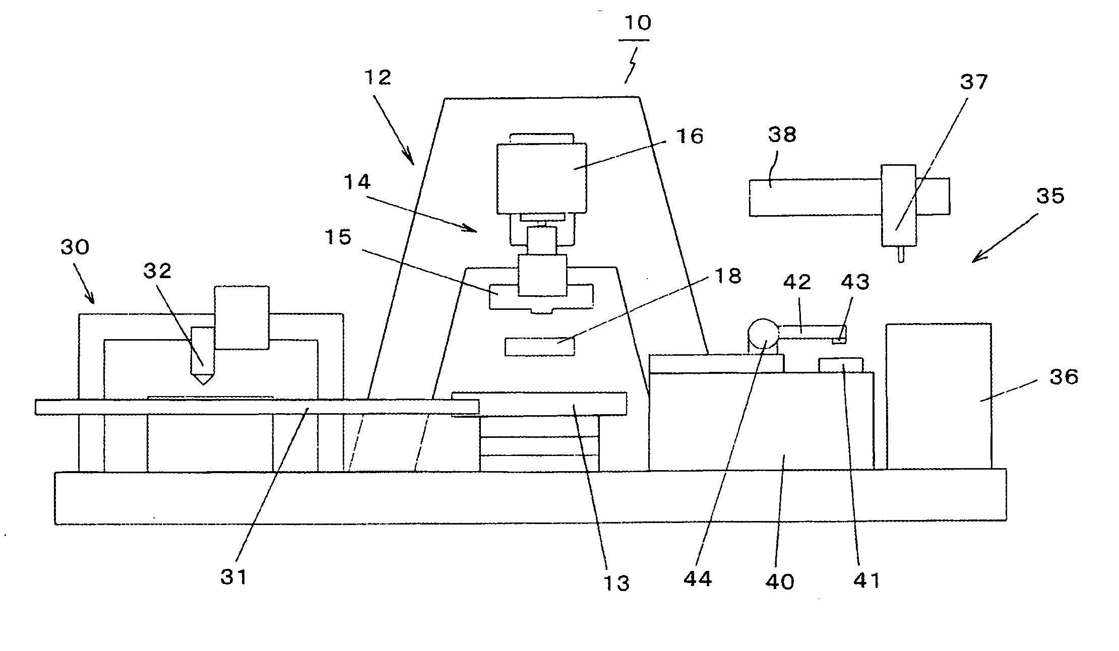
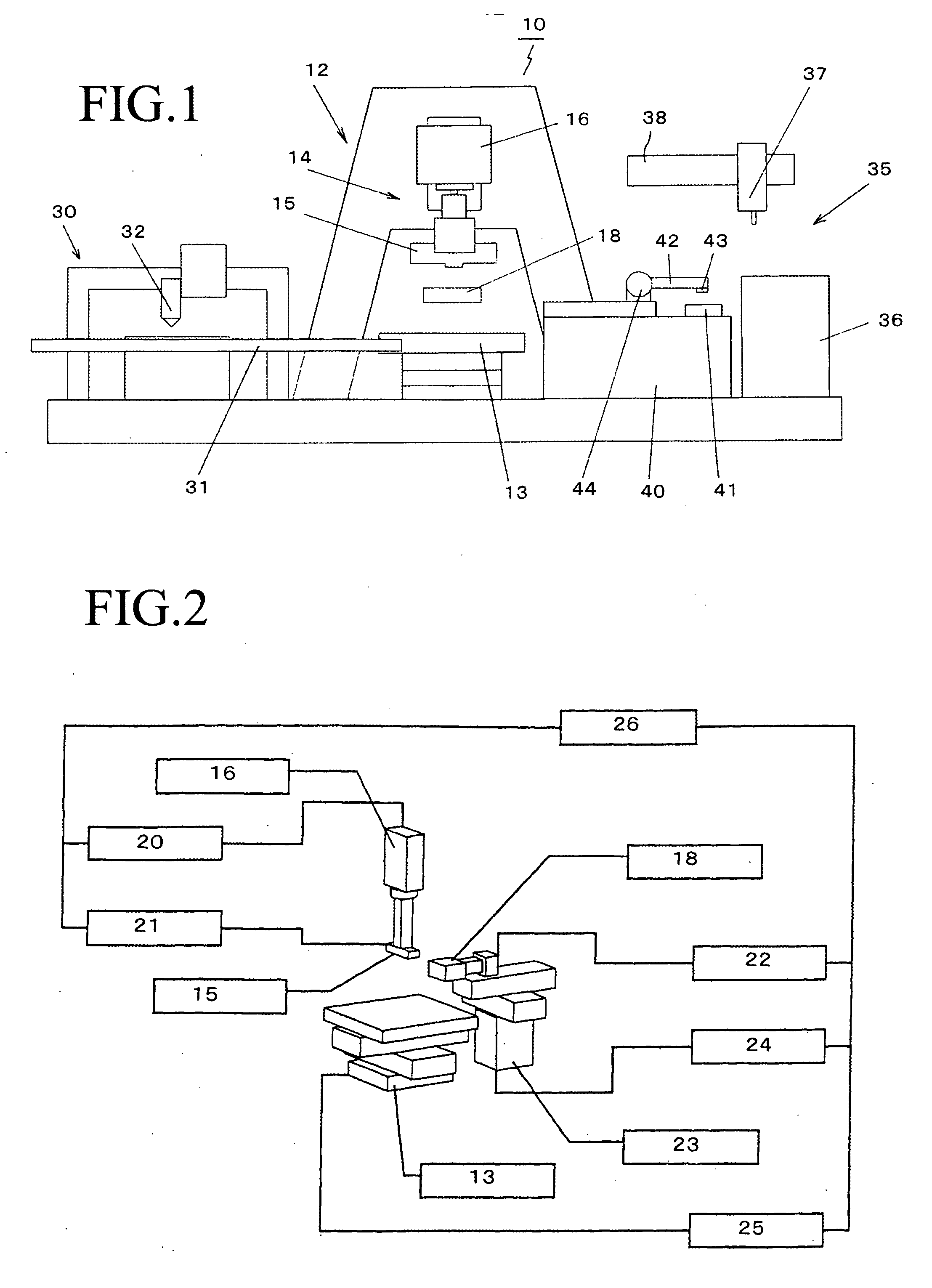
[0039]FIG. 1 is a schematic diagram showing one example of the entire construction of a flip-chip mounting apparatus 10.

[0040] Reference numeral 12 designates an ultrasonic bonding unit. The ultrasonic bonding unit 12 includes a stage 13 onto which a substrate is conveyed and a bonding tool 14 that is disposed above the stage 13, holds a semiconductor chip on a lower surface thereof, and can move relatively toward and away from the stage 13.

[0041] The stage 13 is composed of a well-known XY table and can be moved in a desired direction within a horizontal plane by a driving unit, not shown. The XY table is constructed so as to be capable of being rotated within the horizontal plane about the vertical axis by a rotational driving unit, not shown.

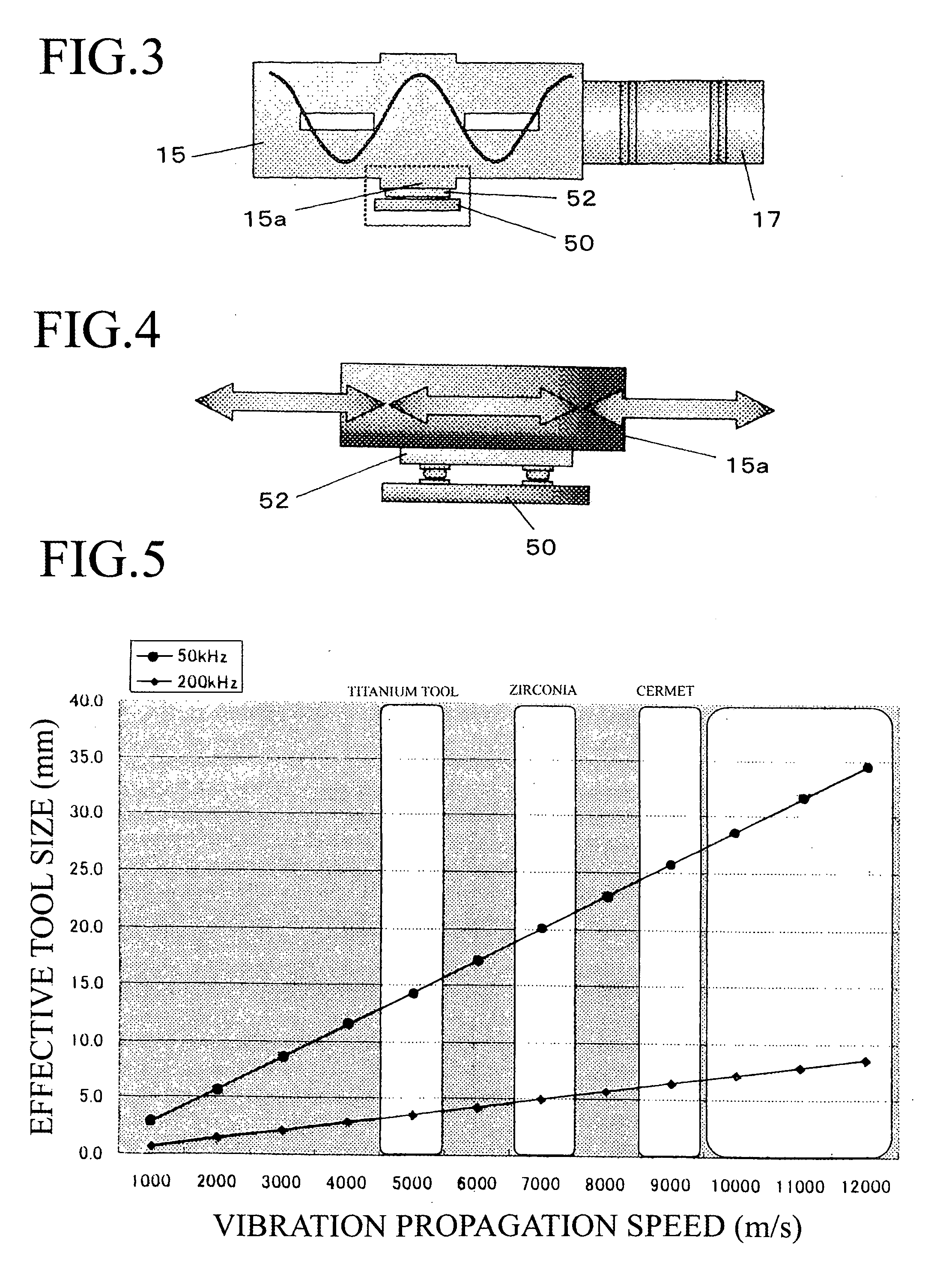
[0042] The bonding tool 14 is composed of a well-known ultrasonic bonding device, and includes a horn 15 for ult...


PUM

PropertyMeasurementUnit
Speedaaaaaaaaaa
Efficiencyaaaaaaaaaa
Elasticityaaaaaaaaaa

Abstract

A method of ultrasonic mounting can increase mounting efficiency by using high-frequency ultrasound and can also mount large semiconductor chips. The method ultrasonically bonds a semiconductor chip 52 to a substrate 50 using an ultrasonic mounting apparatus including a horn 15 that propagates ultrasonic vibration of an ultrasonic vibrator, the horn 15 being made of a ceramic that has a higher vibration propagation speed than metal. The method includes steps of disposing the substrate 50 on a stage 13, disposing the semiconductor chip 52 on the substrate 50, and placing the semiconductor chip 52 in contact with a convex part 15a provided on the horn 15 and applying ultrasonic vibration to bond the semiconductor chip 52 to the substrate 50.

Description

BACKGROUND OF THE INVENTION [0001] 1. Field of the Invention [0002] The present invention relates to a method of ultrasonic mounting that bonds a semiconductor chip to a substrate and an ultrasonic mounting apparatus using the same. [0003] 2. Related Art [0004] When flip-chip bonding and mounting a semiconductor chip on a circuit board, a method is used that places electrode terminals, such as bumps, of the semiconductor chip in contact with electrode terminals, such as pads, of the circuit board and applies ultrasonic vibration to the semiconductor chip to bond the electrode terminals of the semiconductor chip and the circuit board together. [0005] Conventionally, around 50 kHz is used as the frequency of the ultrasound applied to the semiconductor chip. [0006] However, the present inventors have discovered that a large amount of bonding energy is obtained when ultrasound with a high frequency of around 200 kHz is used, which means that the mounting efficiency can be increased. [00...

Claims


Application Information

Patent Timeline
IPC IPC(8): B23K1/06
CPCB23K20/10B23K2201/40H01L2224/16B23K2101/40H01L2224/05573H01L2224/05568H01L2924/00014H01L2224/0554H01L2224/05599H01L2224/0555H01L2224/0556
Inventor KAINUMA, NORIOKIRA, HIDEHIKOKOBAE, KENJIMATSUMURA, TAKAYOSHI
Owner FUJITSU LTD
Why Eureka
Try Eureka