Method and structure for improved LED light output

Active Publication Date: 2006-05-11
AVAGO TECH INT SALES PTE LTD
View PDF5 Cites 23 Cited by
  • Summary
  • Abstract
  • Description
  • Claims
  • Application Information

AI Technical Summary

Benefits of technology

[0003] In accordance with the invention multiple active regions in series separated by tunnel junctions are incorporated into AlGaInN or InGaN LEDs. For a fixed input power, LEDs in accordance with the invention require higher drive voltages but the cur

Problems solved by technology

The effect limits the performance of A

Method used


Image

  • Method and structure for improved LED light output
  • Method and structure for improved LED light output
  • Method and structure for improved LED light output

Examples


Embodiment Construction

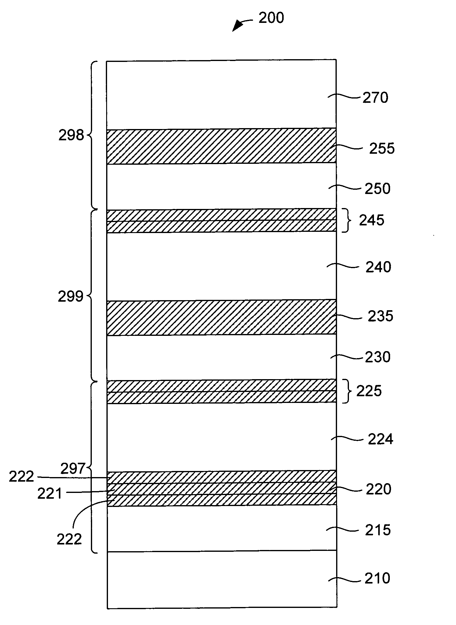
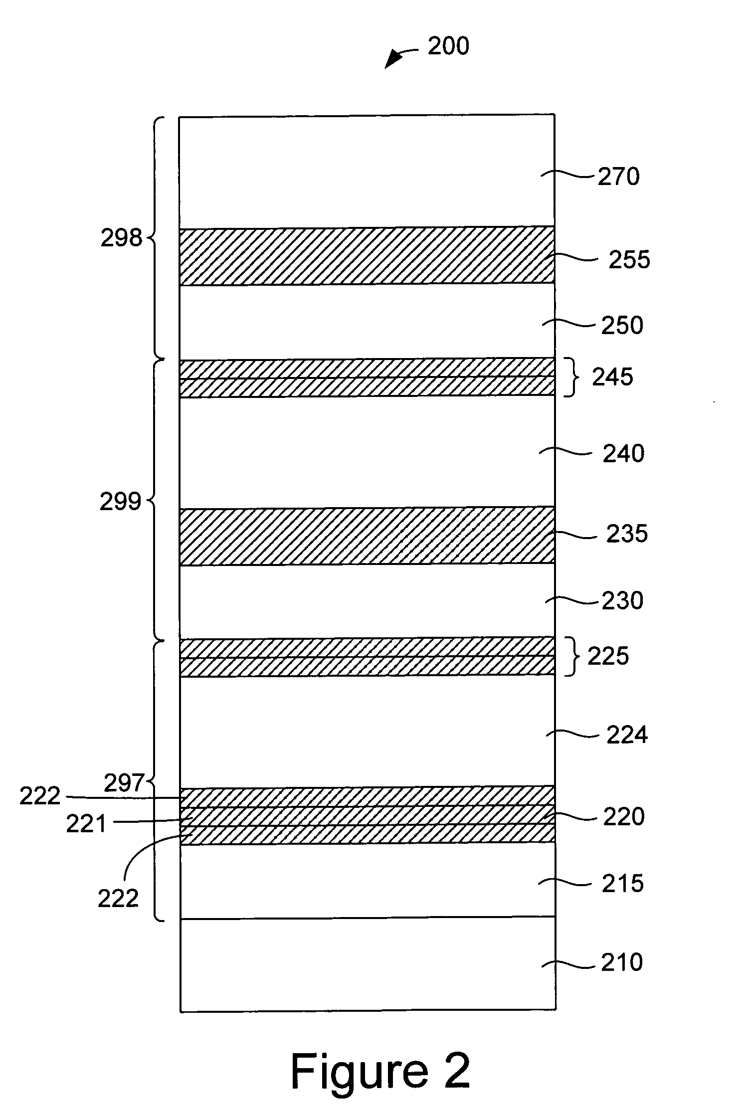
[0009]FIG. 2 shows LED structure 200 in accordance with the invention. N-type (AlxIn(1-x))y Ga(1-y) N cladding layer 215 with x=0, y=0 or x=0 is grown to a typical thickness in the range from about 2 μm to about 5 μm on substrate 210 which is typically Al2O3, SiC GaN, or AlN. Quantum well active region 220, typically including one to ten InGaN quantum wells and typically separated from one another by GaN barrier layers, is grown over AlGaInN cladding layer 215. Growth of quantum well active region 220 is followed by growing p-type AlGaInN cladding layer 224 to a thickness typically in the range from about 0.03 μm to about 0.5 μM thick. Next tunnel junction 225 is formed by growing heavily doped p++ AlGaInN layer 226 to a thickness typically in the range from about 100 to 500 angstroms, followed by growing heavily doped n++ AlGaInN layer 227 to a thickness typically in the range from about 100 to 500 angstroms. P++ AlGaInN layer 226 is heavily p doped, typically with magnesium to a c...


PUM


Abstract

The efficiency of LEDs is increased by incorporating multiple active in series separated by tunnel junction diodes. This also allows the LEDs to operate at longer wavelengths.

Description

BACKGROUND OF THE INVENTION [0001] The operating efficiency of light emitting diodes (LEDs) may be improved in a number of ways. These include improvements in the quality of the semiconductor layers and the design of the structure to maximize coupling of light out of the LED. [0002] The operating efficiency of LEDs based on AlGaInN or InGaN decreases as the net drive current is increased as is shown in graph 110 of FIG. 1 for a green GaInN LED. This effect exists in addition to the well-known effect in LEDs where efficiency decreases due to heating brought on by increases in the drive current. The effect limits the performance of AlGaInN or InGaN at high drive currents. Additionally, for AlGaInN or InGaN LEDs, a wavelength shift to shorter wavelengths occurs as the current increases. BRIEF SUMMARY OF THE INVENTION [0003] In accordance with the invention multiple active regions in series separated by tunnel junctions are incorporated into AlGaInN or InGaN LEDs. For a fixed input powe...

Claims


Application Information

Patent Timeline
IPC IPC(8): H01L33/00H01L33/08
CPCH01L33/08
Inventor LESTER, STEVEN D.
Owner AVAGO TECH INT SALES PTE LTD
Why Eureka
Try Eureka