Chip resistor, process for producing the same, and frame for use therein

a technology of chip resistors and resistors, which is applied in the field of chip resistors, can solve the problems of increasing the overall thickness the increase of the manufacturing cost of the chip resistor b

Active Publication Date: 2006-05-11
ROHM CO LTD
View PDF6 Cites 30 Cited by
  • Summary
  • Abstract
  • Description
  • Claims
  • Application Information

AI Technical Summary

Benefits of technology

[0010] An object of the present invention is to provide a chip resistor and a manufacturing method thereof which can solve or suppress the problems described above. Another object of the present invention is to provide a frame which is suitable for use in the manufacture of such a chip resistor.

Problems solved by technology

However, when such means are employed, the overall thickness of the chip resistor B increases, the amount of the metallic plate 91′ that must be cut to form the void portion 93 increases, and as a result, the manufacturing cost of the chip resistor B rises.

Method used


Image

  • Chip resistor, process for producing the same, and frame for use therein
  • Chip resistor, process for producing the same, and frame for use therein
  • Chip resistor, process for producing the same, and frame for use therein

Examples


Embodiment Construction

[0083] Preferred embodiments of the present invention will be described below specifically, with reference to the drawings.

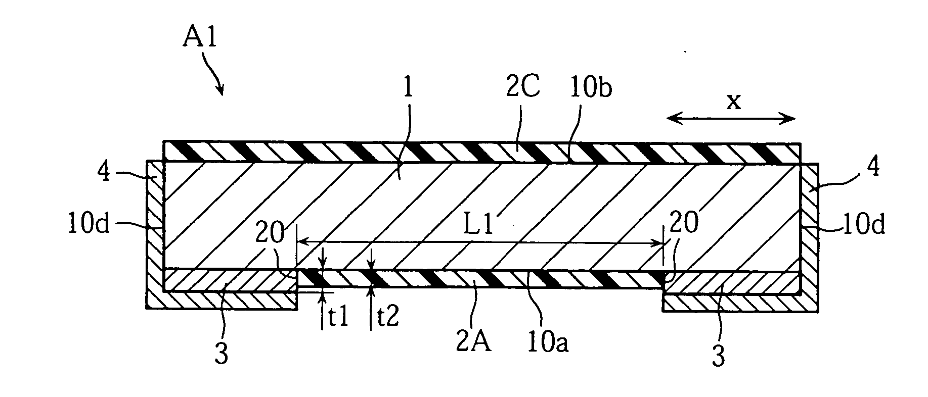
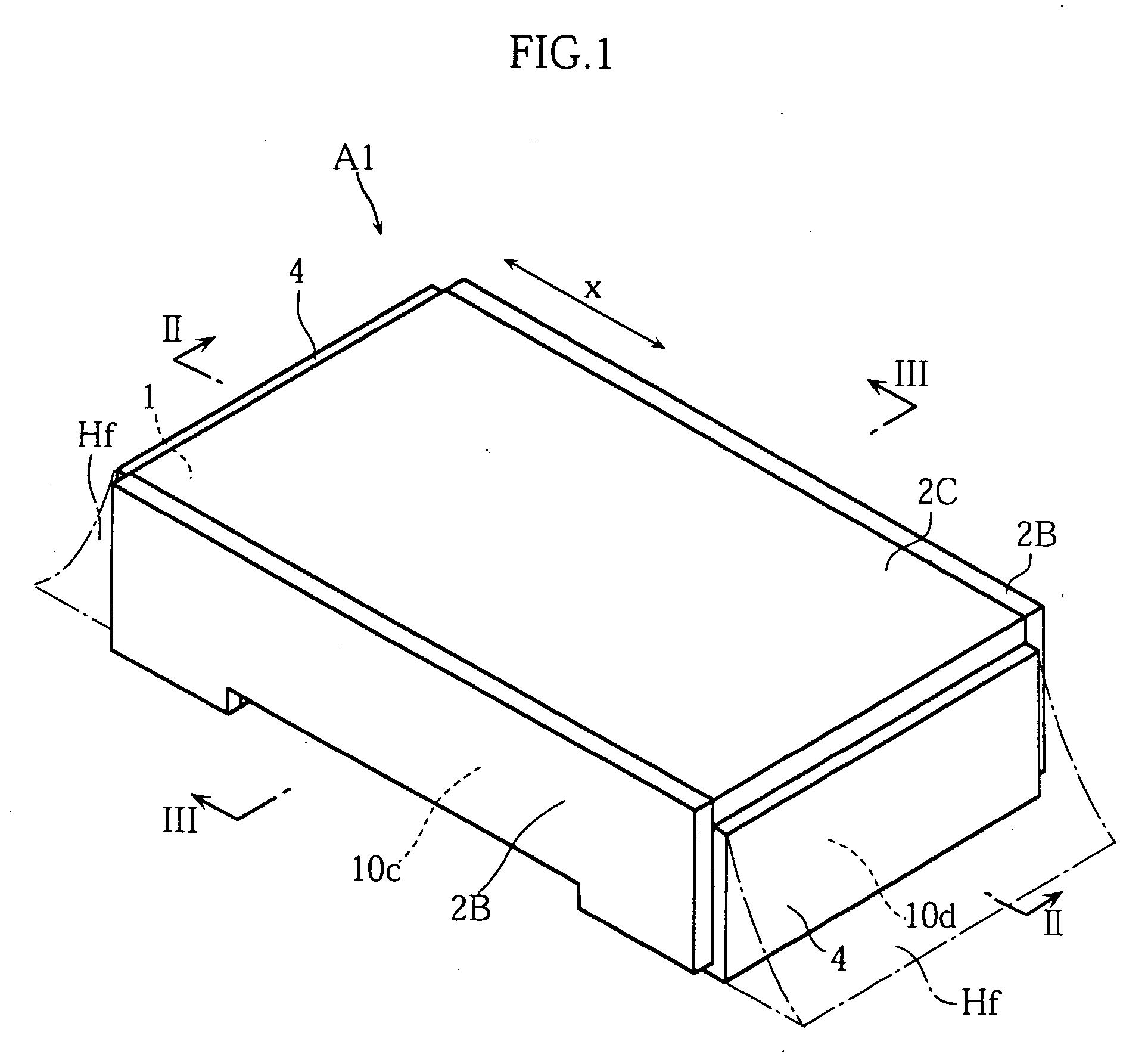
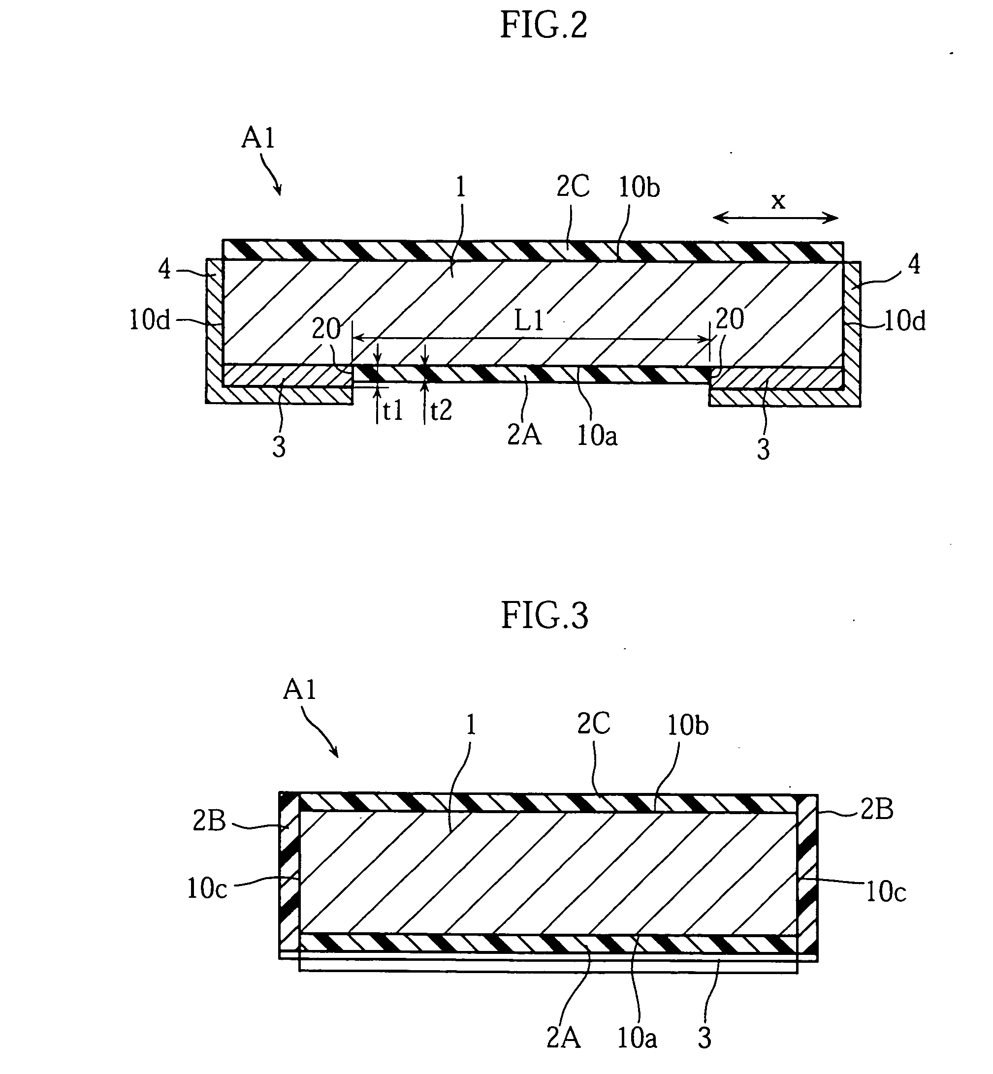
[0084] FIGS. 1 to 4 show an example of the chip resistor according to the present invention. As is shown clearly in the drawings, a chip resistor A1 of this embodiment comprises a resistor 1, first through third insulation layers 2A to 2C, a pair of electrodes 3, and a pair of solder layers 4.

[0085] The resistor 1 is formed from metal in a rectangular chip form when seen from above. Specific examples of the materials used for the resistor 1 include an Ni—Cu alloy, a Cu—Mn alloy, and an Ni—Cr alloy. Note, however, that the material is not limited to these examples, and a material having a resistivity which is suited to the size and target resistance value of the chip resistor A1 may be selected appropriately.

[0086] The first through third insulation layers 2A to 2C are all resin films formed from epoxy resin or the like, and are formed by thick film printing, ...


PUM


Abstract

A chip resistor (A1) comprises a first insulation layer (2A) covering the regions between a plurality of electrodes (3) on a rear surface (10a) of a resistor (1), and a second insulation layer covering a pair of side faces of the resistor (1). Inadvertent adhesion of solder to an improper part of the resistor (1) can thereby be eliminated. A solder layer (4) is preferably formed on a pair of end faces (10d) of the resistor (1). In so doing, a solder fillet can be formed appropriately.

Description

TECHNICAL FIELD [0001] The present invention relates to a chip resistor, a manufacturing method thereof, and a frame used in this manufacturing method. BACKGROUND ART [0002]FIG. 37 shows an example of a conventional chip resistor (see Japanese Unexamined Patent Application Publication 2002-57009, for example). A chip resistor B shown in the drawing is constituted such that a pair of electrodes 91 is provided on a lower surface 90b of a metallic chip-form resistor 90. The electrodes 91 are separated from each other by a void portion 93. A solder layer 92 is formed on the lower surface of each electrode 91 as means for improving solder ability during mounting. [0003] This chip resistor B is manufactured using a method such as that shown in FIGS. 38A to 38E. First, as shown in FIG. 38A, two metallic plates 90′, 91′ are prepared as the materials for the resistor 90 and electrodes 91, and then, as shown in FIG. 38B, the metallic plate 91′ is superposed on the lower surface of the metalli...

Claims


Application Information

Patent Timeline
Patent Type & Authority Applications(United States)
IPC IPC(8): H01L29/00H01C1/144H05K3/34
CPCH01C1/144H05K3/3442
Inventor TSUKDA, TORAYUKIMIWA, TADATOSHI
Owner ROHM CO LTD
Why Eureka
Try Eureka