Thin film transistor tester and corresponding test method

a thin film transistor and tester technology, applied in the direction of electrical testing, measurement devices, instruments, etc., can solve the problems of insufficient circuit built therewith to be used as a pixel circuit, damage to tft arrays, and inability or very difficult to test tft electrical characteristics

Inactive Publication Date: 2006-05-11
GOOGLE LLC
View PDF12 Cites 7 Cited by
  • Summary
  • Abstract
  • Description
  • Claims
  • Application Information

AI Technical Summary

Benefits of technology

[0014] The tester and test method of a TFT array substrate of the present invention are capable of testing the electrical characteristics of the TFT without having adverse effects (contamination, destruction, etc.) on the TFT, by supplying an ion flo...

Problems solved by technology

Therefore, any circuit built therewith is inadequate to be used as a pixel circuit.
As a result, at the stage where the TFT array step ends, it is impossible or very difficult to test the TFT electrical characteristics.
Since fluctuations of the TFT electrical characteristics seriously and adversely affect the image quality of the AMOLED display, there is a strong demand for performing the parametric tests at the TFT array stage.
Since the TFT array requires a full immersion in the solution, the method described is not actually used in a manufacturing line.
Therefore, there is a danger that the TFT array will be damaged when forming the c...

Method used


Image

  • Thin film transistor tester and corresponding test method
  • Thin film transistor tester and corresponding test method
  • Thin film transistor tester and corresponding test method

Examples


Embodiment Construction

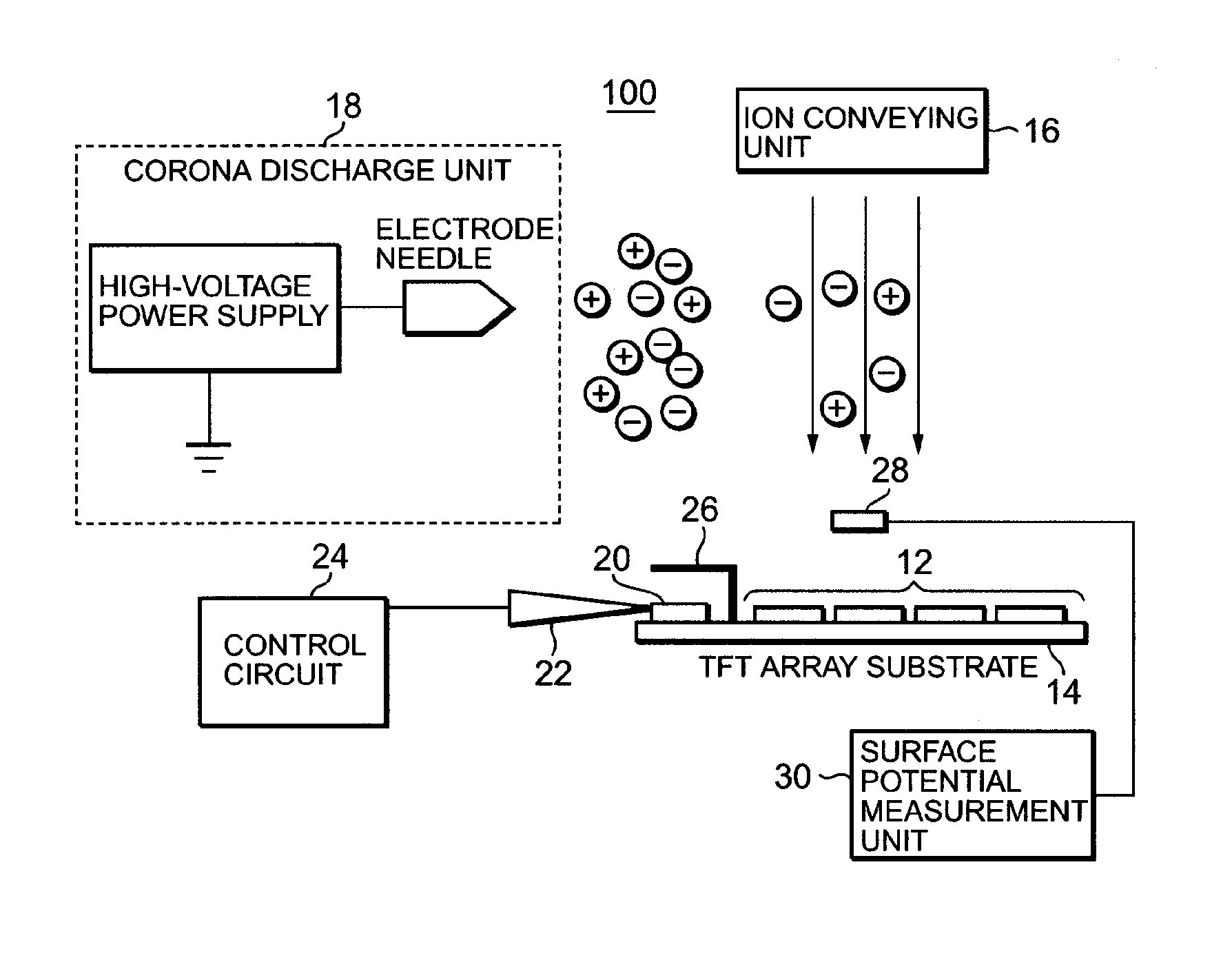
[0036] Referring now to FIG. 1, there is shown a diagram illustrating an N-channel TFT used as the device to be tested. Gate 1 of TFT 10 is connected to a driving voltage line 5. Either source or drain 2 is attached to current detection line 6, while 3 is connected to an open electrode 4. Since electrode 4 is open, TFT 10 does not operate even when a driving voltage is applied to gate 1. Moreover, the driving current cannot be detected from line 6. In the present invention, the open electrode 4 is irradiated by an ion flow 7. The ion flow 7 operates as a TFT voltage source (current source). When an operating voltage Vg is supplied to gate 1, TFT 10 turns on. When the TFT turns on, an operating current Id is detected by line 6. Furthermore, the surface potential Vd of electrode 4 is measured. The electrical characteristics of TFT 10 are checked from the driving voltage Vg, the operating current Id, or the surface potential Vd and the potential Vs of the current detection line, to fur...


PUM


Abstract

To test electrical characteristics of a Thin Film Transistor (TFT) with a source or drain terminal left open and exposed, using a non-contact current source and protecting the TFTs from adverse effects, such as contamination, destruction, and the like. A tester 100 is provided to test a TFT array substrate 14, the tester including ion flow supply devices 16 and 18 for supplying an ion flow onto the surface of a substrate 14. Thereon, an array 12 of TFTs is formed, each TFT being connected to an electrode having a source or a drain left open and exposed; a control circuit 24 for supplying an operating voltage to a gate electrode of the TFT to be tested in the array; and a measurement circuit 24 for measuring an operating current via the testing TFT source or drain that remain in a non open state.

Description

BACKGROUND OF THE INVENTION [0001] The present invention generally relates to a Thin Film Transistor (TFT) tester and a TFT test methodology, and more particularly, to an apparatus and method for testing the operating characteristics of a TFT array using a non-contact voltage or current source. [0002] The steps for manufacturing an organic light emitting diode (OLED) display (hereinafter referred to as an AMOLED display) of an active matrix are roughly divided into a ‘TFT array step’ of forming a TFT array for driving purposes, and a subsequent ‘cell step’ of forming the OLED on the array. At the stage at which the formation of the TFT array ends, the OLED which consists of a light emitting material, is not made on the TFT array substrate. Therefore, any circuit built therewith is inadequate to be used as a pixel circuit. Thus, only when the TFT array is formed, a drain or source of the TFT that is connected to an exposed pixel electrode is brought into an open state. Therefore, any...

Claims


Application Information

Patent Timeline
IPC IPC(8): G01R31/00
CPCG09G3/006
Inventor IMURA, KENICHINAKANO, DAIJUSAKAGUCHI, YOSHITAMI
Owner GOOGLE LLC
Why Eureka
Try Eureka