
Optical element housing package
- Summary
- Abstract
- Description
- Claims
- Application Information
AI Technical Summary
Benefits of technology
Problems solved by technology
Method used
Image

Examples
Embodiment Construction
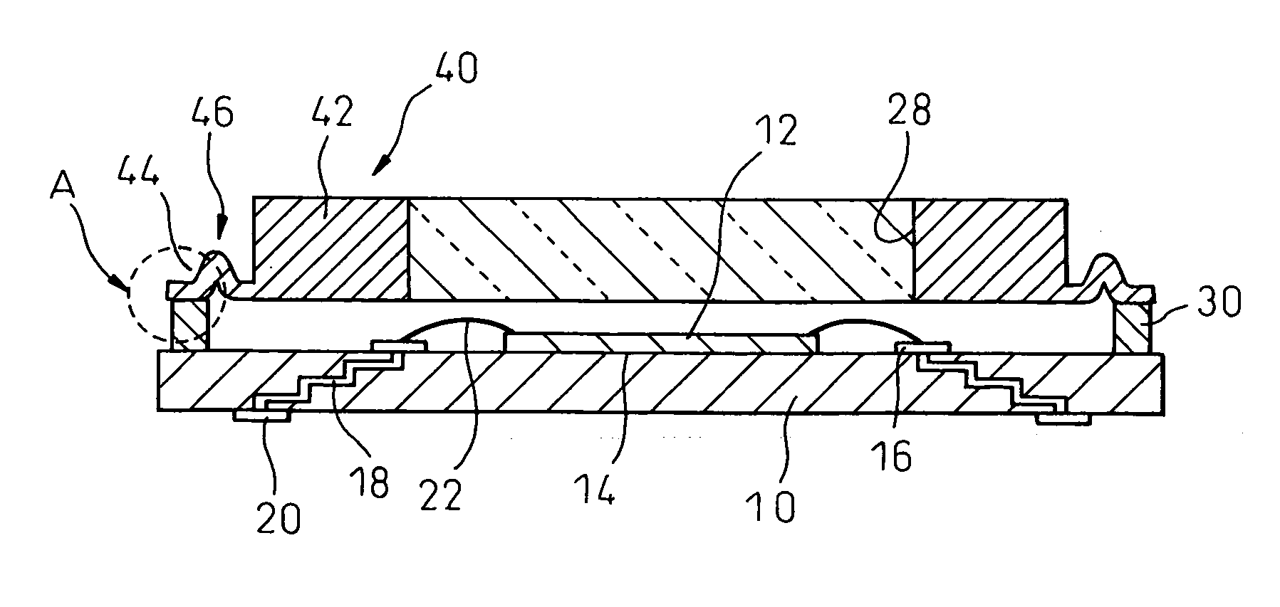
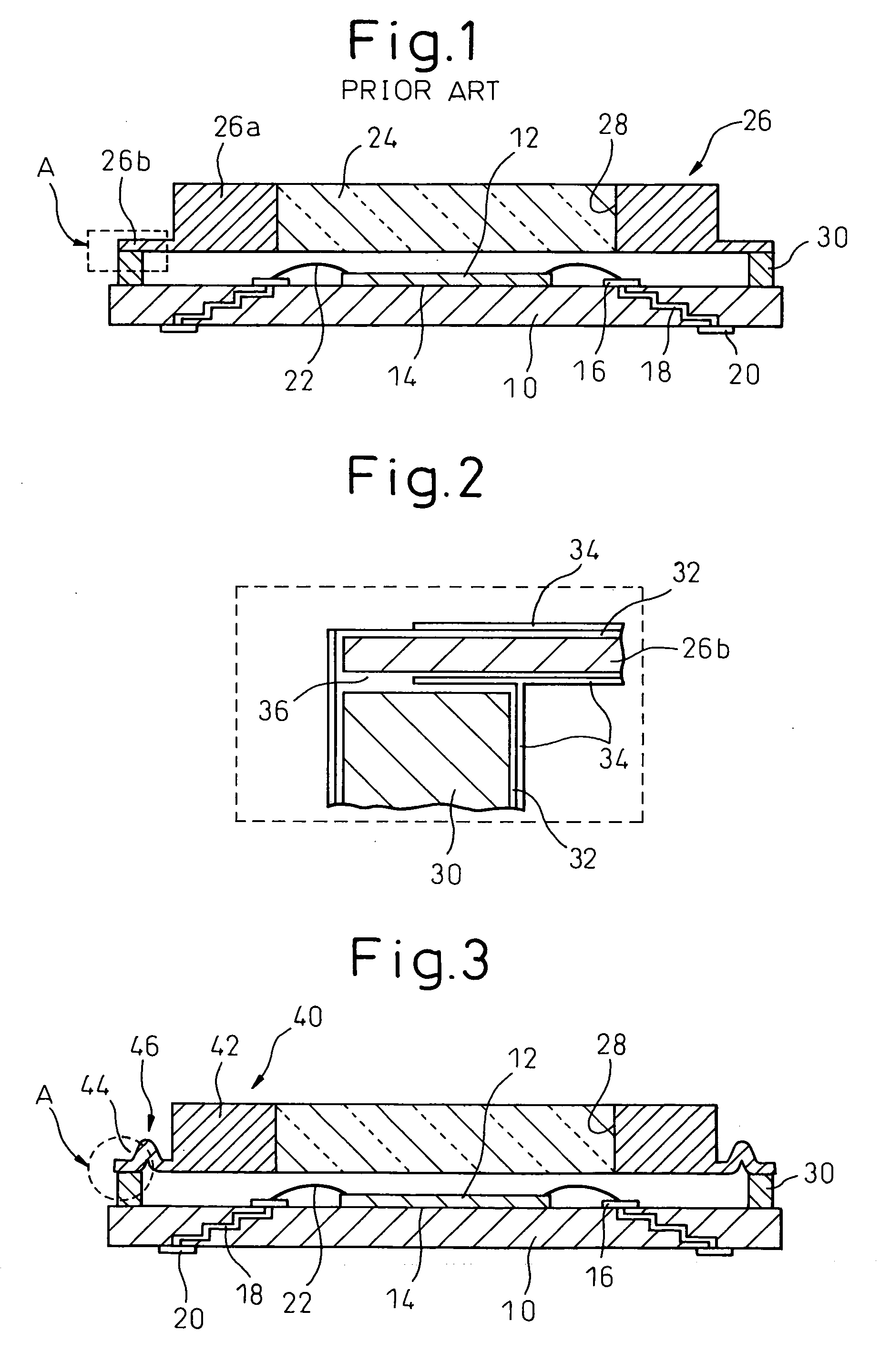
[0018] An embodiment of the present invention will be explained, in detail, below with reference to the drawings and will be compared to the prior art.
[0019]FIG. 1 is a cross-sectional view showing a structure of a DMD (Digital Micromirror Device) package as an example of a known optical element housing package.
[0020] On an upper surface of an insulation substrate made of ceramic, etc., a element mounting area 14 for mounting an optical element 12, for example, a micromirror, is provided. A large number of bonding pads 16 are provided at the periphery of the element mounting area 14 on the upper surface of the insulation substrate 10. Each pad 16 is connected to an external connection pad 20 on the lower surface of the insulation substrate 10, through inside wiring 18 of the insulation substrate 10.
[0021] After the optical element 12 is mounted on the element mounting area 14 of the insulation substrate 10, electrode terminals of the optical element 12 and the bonding pads 16 on ...
PUM
 Abstract
Description
Claims
Application Information