Semiconductor memory device

a memory device and semiconductor technology, applied in the field of semiconductor memory devices, can solve the problems of low confidentiality, disadvantageous in general low security, and employing such encryption schemes, and achieve excellent read performan

Active Publication Date: 2006-05-18
NINTENDO CO LTD +1
View PDF16 Cites 41 Cited by
  • Summary
  • Abstract
  • Description
  • Claims
  • Application Information

AI Technical Summary

Benefits of technology

[0010] The exemplary illustrative non-limiting implementation has the plurality of operating modes different in security strength, and operates while changing between these operating modes to provide the semiconductor memory device with enhanced security strength and excellent read performance.
[0014] It is therefore an object of the exemplary illustrative non-limiting implementation to provide a semiconductor memory having a high-level security function and excellent read performance in consideration for a balance between the strength of security and data transfer efficiency.

Problems solved by technology

Japanese Patent Application Laid-Open No. 9-106690, however, discloses a security method using a scrambling scheme which is advantageous in high data transfer efficiency but is disadvantageous in generally low strength of security.
Japanese Patent Application Laid-Open No. 2001-35171 or Japanese Patent Application Laid-Open No. 7-219852 employs a one-step logic operation by means of the logic circuit, which features fast processing but is disadvantageous in low confidentiality because it is easy to analyze the security method if what logic circuit is used is known.
The security method employing such an encryption scheme, however, is disadvantageous in low data transfer efficiency although having the advantage of its high strength of security.

Method used


Image

  • Semiconductor memory device
  • Semiconductor memory device
  • Semiconductor memory device

Examples


Embodiment Construction

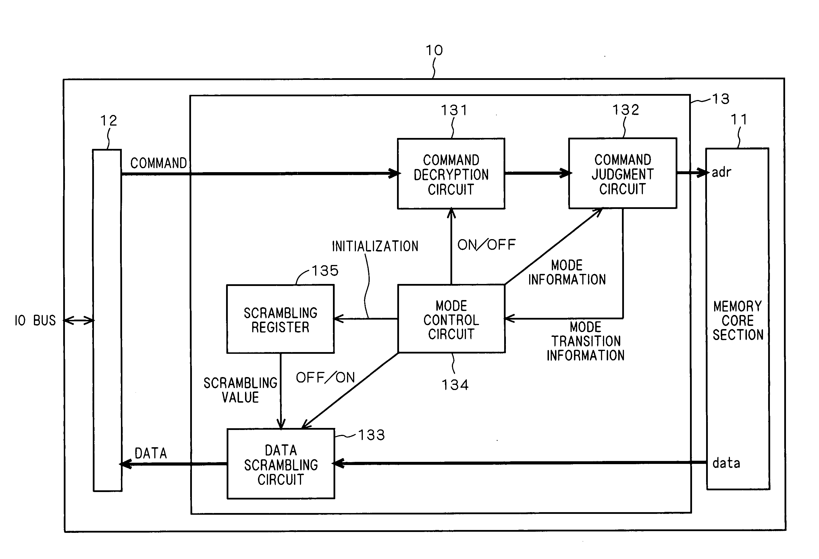
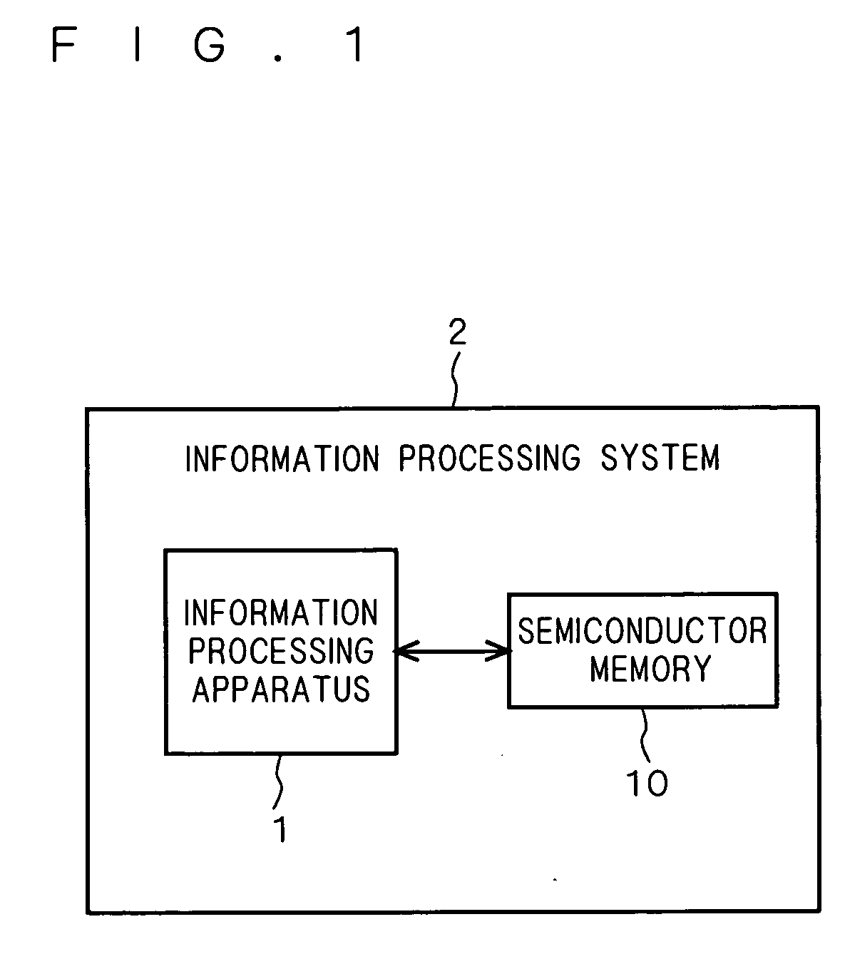
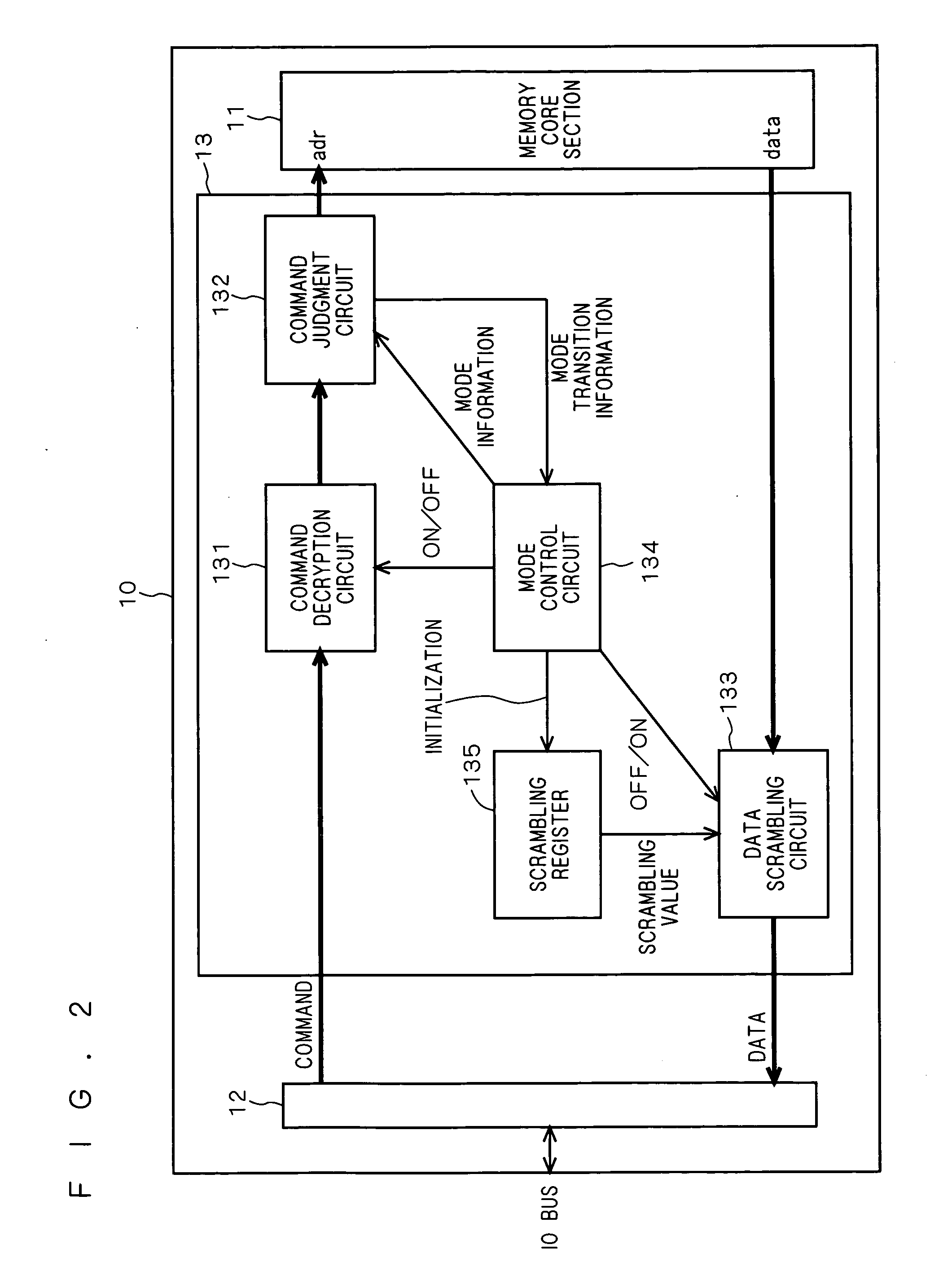
[0025] Exemplary illustrative non-limiting implementations will now be described with reference to the drawings. FIG. 1 is a diagram showing a relationship between an exemplary illustrative non-limiting semiconductor memory device 10 and an information processing apparatus 1 to which the exemplary semiconductor memory device 10 is applied. In the exemplary illustrative non-limiting implementation, the semiconductor memory device (hereinafter referred to simply as a “semiconductor memory”) 10 is a nonvolatile memory (for example, a ROM, a flash memory or the like) removable from the body of the information processing apparatus 1. The semiconductor memory 10 fixedly stores therein various data including a program, image data, music data and the like the confidentiality of which must be protected from unauthorized duplication or unauthorized reading. The information processing apparatus 1 includes a CPU and a RAM, and executes a variety of information processing depending on the data s...


PUM


Abstract

A semiconductor memory includes a memory control section and a memory core section. A command judgment circuit in the memory control section changes the operating mode of the semiconductor memory in response to a command sent from a controller of an information processing apparatus. In a first mode, a decryption process is performed in a command decryption circuit, and data outputted from the memory core section is not scrambled. In a second mode, the decryption process is not performed in the command decryption circuit, and the command outputted from the memory core section is scrambled.

Description

CROSS-REFERENCES TO RELATED APPLICATIONS [0001] This application is a U.S. utility application claiming priority to U.S. Provisional Application No. 60 / 627,908 filed 16 Nov. 2004 and JP 2004-330570 filed 15 Nov. 2004, the entire contents of each of which are hereby incorporated by reference.FIELD [0002] The technology herein relates to a semiconductor memory device and, more particularly, to the security of various data stored in a semiconductor memory. BACKGROUND AND SUMMARY [0003] An information processing apparatus has been known which includes a semiconductor memory removable therefrom and which operates using data containing a program stored in the semiconductor memory. A variety of mechanisms have been proposed to provide the security of the data stored in this semiconductor memory. [0004] Japanese Patent Application Laid-Open No. 9-106690 (1997) discloses a technique for scrambling data outputted from a semiconductor memory by the use of key data to provide the security of th...

Claims


Application Information

Patent Timeline
Patent Type & Authority Applications(United States)
IPC IPC(8): G06F12/14
CPCG06F12/1408
Inventor UMEZU, RYUJIYAMAGUCHI, IKUO
Owner NINTENDO CO LTD
Why Eureka
Try Eureka