Column averaging/row binning circuit for image sensor resolution adjustment in lower intensity light environment

a resolution adjustment and image sensor technology, applied in the field of image sensor array processing, can solve the problems of loss of spatial resolution, loss of image quality of pixel sub-sampling, and high decimation ratio, and achieve the effects of low light level, high image quality, and high image quality

a resolution adjustment and image sensor technology, applied in the field of image sensor array processing, can solve the problems of loss of spatial resolution, loss of image quality of pixel sub-sampling, and high decimation ratio, and achieve the effects of low light level, high image quality, and high image quality

US20060108506A1Active Publication Date: 2006-05-25YOULIZA GEHTS LIABILITY

Image

  • Column averaging/row binning circuit for image sensor resolution adjustment in lower intensity light environment
  • Column averaging/row binning circuit for image sensor resolution adjustment in lower intensity light environment
  • Column averaging/row binning circuit for image sensor resolution adjustment in lower intensity light environment

Examples


Embodiment Construction

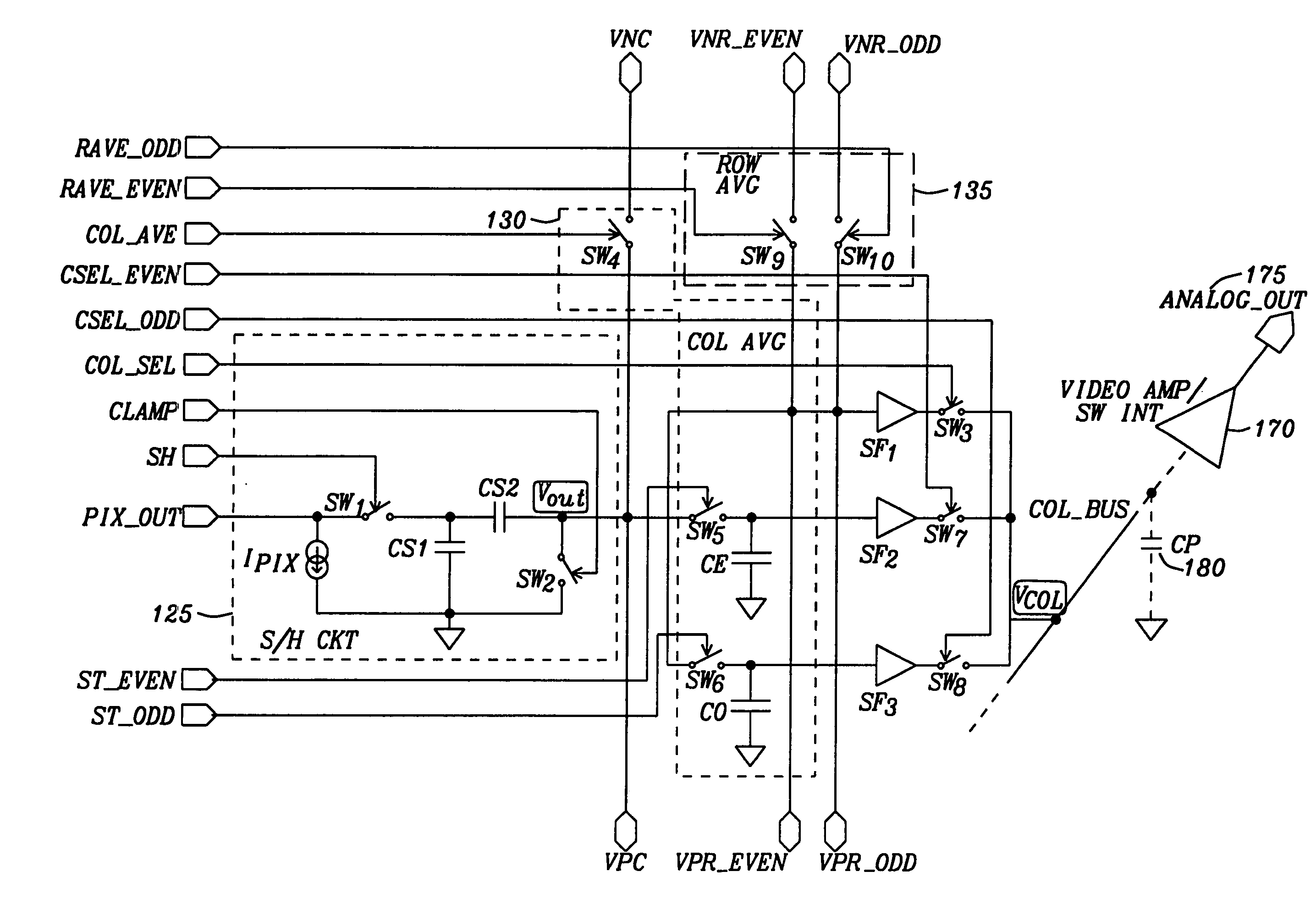
[0113] The CMOS active pixel sensor array of this invention achieves high spatial resolution in the analog domain and high image quality at low light level by a horizontal (column) pixel averaging and vertical (row) pixel binning approach for Bayer patterned pixel array. Additionally, the CMOS active pixel sensor array of this invention achieves high spatial resolution in the analog domain and high image quality at high light level by a horizontal (column) and vertical (row) pixel averaging approach for Bayer patterned pixel array. The advantages of the CMOS active pixel sensor array of this invention are a simple analog column sample and hold circuit; a reduced pixel output rate for decimated image to achieve low power operation; no additional on-chip memory required; and a scalability to any pixel array decimation ratio.

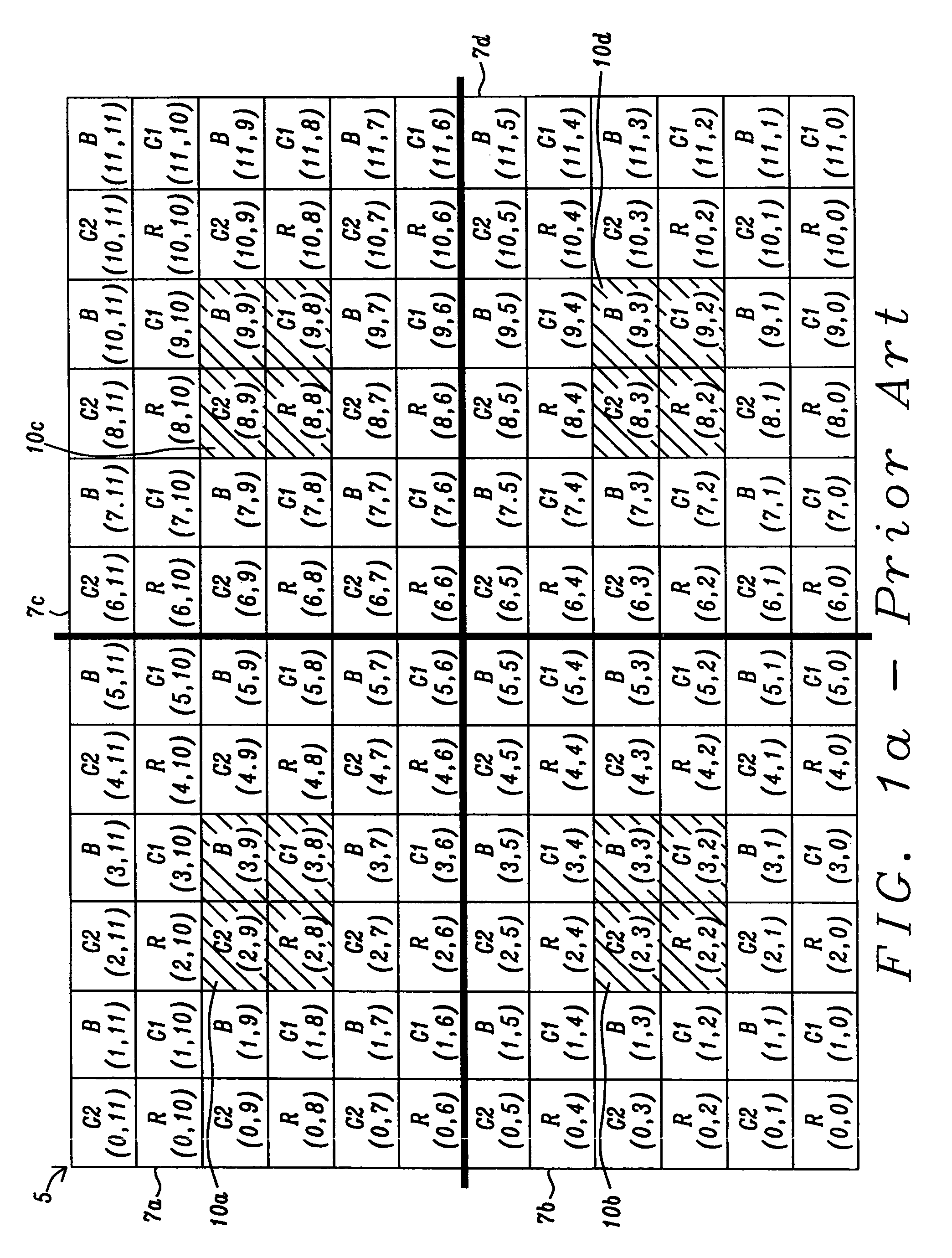
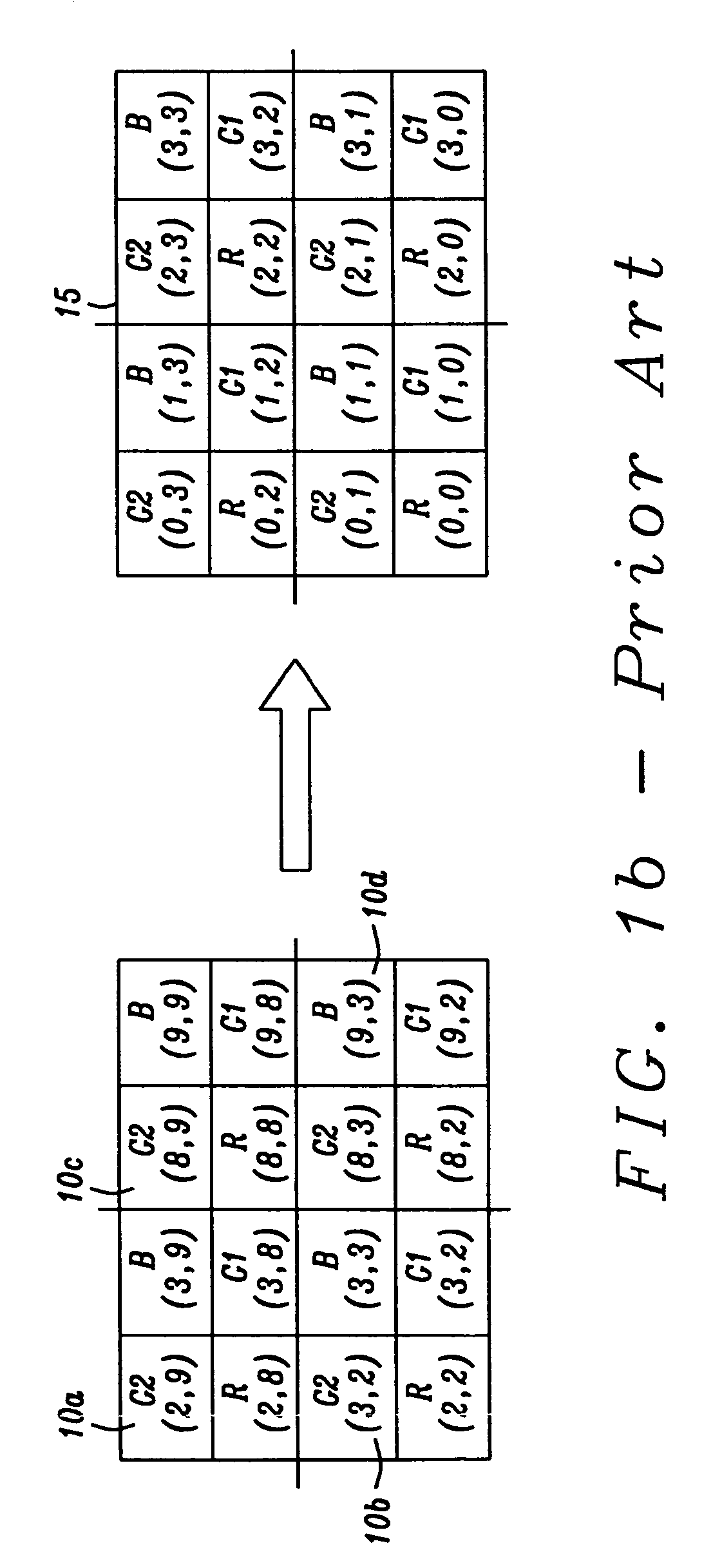
[0114] As shown in FIG. 5, an array of color CMOS APS image sensors 100 is arranged in rows and columns. The array 100 is formed of three types of CMOS APS image ...


PUM


Abstract

A photo-sensor image resolution adjustment apparatus is in communication with an array of image photo-sensors that are organized in columns and rows and have multiple sensor types arranged in a pattern such as a Bayer pattern to detect light. The photo-sensor image resolution adjustment apparatus has a photo-sensor array decimation circuit to partition the array of image photo-sensors into a plurality of sub-groups. A column averaging circuit averages the light conversion electrical signals from common color photo-sensors within the sub-groups. A row averaging circuit averages the common color adjacent light conversion electrical signals from color adjacent rows within the sub-groups in high light intensity condition. In low light conditions, a row binning circuit integrates the common color adjacent light conversion electrical signals from color adjacent rows within the sub-groups.

Description

RELATED PATENT APPLICATIONS [0001]โ€œPixel Binning / Averaging Approach on Large Format Color, CMOS Image Sensor Decimation,โ€ Ser. No. ______, Filing Date ______, assigned to the same assignee as this invention. [0002]โ€œA Column Averaging / Row Averaging Circuit for Image Sensor Resolution Adjustment in High Intensity Light Environment Pixel,โ€ Ser. No. ______, Filing Date ______, assigned to the same assignee as this invention.BACKGROUND OF THE INVENTION [0003] 1. Field of the Invention [0004] This invention relates generally to image sensor array processing. More particularly, this invention relates to circuits and methods for adjusting resolution of image sensors. Even more particularly, this invention relates to circuits and methods for adjusting resolution of image sensors by decimating the addressing of the image sensors into sub-groups of the array of the image sensor, averaging the columns of each of the sub-groups of the image sensor, and selectively averaging in a high intensity l...

Claims


Application Information

Patent Timeline
25 May 2006
Publication
US20060108506A1
IPC
H01L27/00; H04N23/40; H04N25/00
CPC
H04N3/1562; H04N9/045; H04N25/46; H04N25/76; H04N25/78
Inventors
YANG, GUANG; DOSLUOGLU, TANER