Thermal management of surface-mount circuit devices on laminate ceramic substrate

a technology of laminate ceramic and circuit devices, which is applied in the direction of printed circuit aspects, electrical apparatus construction details, lighting and heating apparatus, etc., can solve the problems that the thermal management of power circuit devices cannot be improved by the use of metal-containing ceramic layers, and the ltcc substrate is also electrically conductive, etc., to achieve the effect of improving the thermal management of power circuit devices mounted

Inactive Publication Date: 2006-05-25
DELPHI TECH INC
View PDF19 Cites 112 Cited by
  • Summary
  • Abstract
  • Description
  • Claims
  • Application Information

AI Technical Summary

Benefits of technology

This patent describes a special circuit board made up of multiple layers of ceramic that help manage heat better for certain electronic components on it.

Problems solved by technology

This patent discusses improving thermal management of electronic circuits, specifically power integrated circuits mounted on low temperature co-fired ceramic substrates. The technical problem addressed is how to increase heat transfer from the circuit component to a heat sink without compromising the integrity or functionality of other parts of the system. Current solutions involving thermal vias face limitations including poor heat spreading and insufficient cooling of certain types of circuit elements. There is a desire for more effective methods of managing heat generation in power electronics while utilizing advanced packaging technologies like LTCC.

Method used


Image

  • Thermal management of surface-mount circuit devices on laminate ceramic substrate
  • Thermal management of surface-mount circuit devices on laminate ceramic substrate
  • Thermal management of surface-mount circuit devices on laminate ceramic substrate

Examples


second embodiment

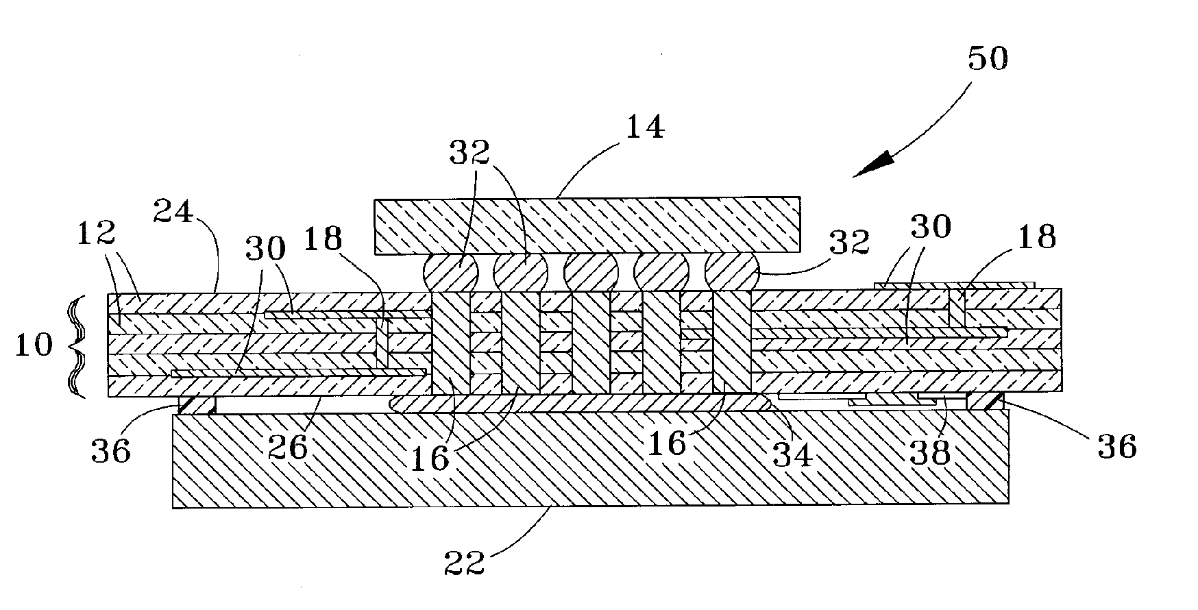
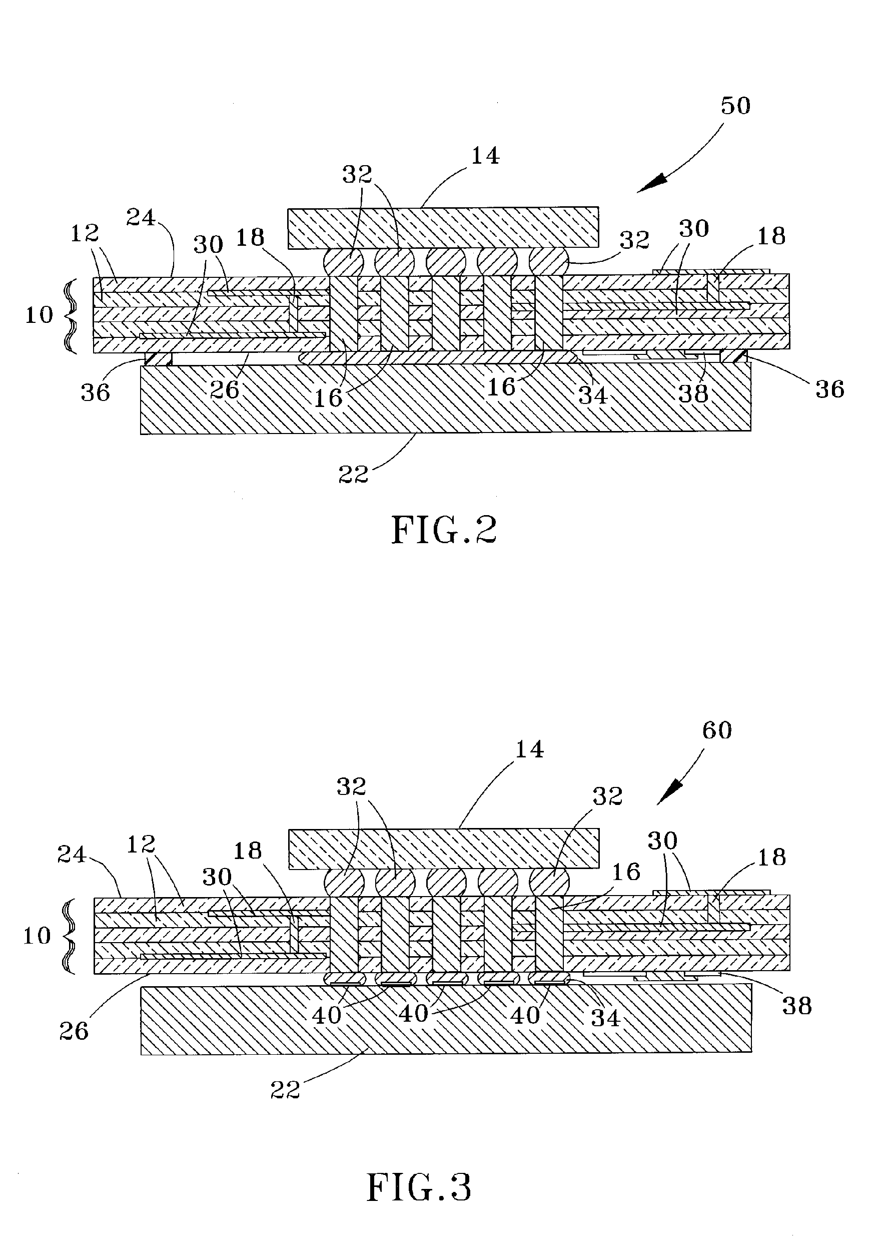
[0020]FIG. 3 depicts a circuit board assembly 60 in accordance with the invention in which, for convenience, corresponding components are identified with the same reference numbers as those used in FIG. 2. As such, a power flip chip 14 is mounted on an LTCC substrate 10 made up of multiple ceramic layers 12. The embodiment of FIG. 3 differs in one aspect from FIG. 2 by the substitution of a nonmetallic (nonelectrically-conductive) heat sink 22 in FIG. 3 for the metallic (electrically-conductive) heat sink 22 of FIG. 2. Another difference apparent from FIG. 3 is the use of multiple solder bumps 34 in FIG. 3 instead of the single solder layer 34 of FIG. 2 to bond the heat sink 22 to the substrate 10. As with the embodiment of FIG. 2, the solder material for the solder bumps 34 is preferably a lower-melting material composition than the solder material used to form the solder bumps 32, so that reflowing the solder bumps 34 to attach the heat sink 22 does not result in reflowing of the ...

third embodiment

[0022] Finally, FIG. 4 depicts a circuit board assembly 70 in accordance with the invention in which, again for convenience, corresponding components are identified with the same reference numbers as those used in FIG. 2. As such, the assembly 70 includes an LTCC substrate 10 made up of multiple ceramic layers 12, a power flip chip 14 on one surface 24 of the substrate 10, and a heat sink 22 attached to the opposite surface 26 of the substrate 10. As in FIG. 2, the heat sink 22 is formed of an electrically-conductive material, such as aluminum. The embodiment of FIG. 4 differs in several aspects from the embodiment of FIG. 2. For example, the thermal vias 16 for the flip-chip 14 are physically and thermally coupled to the heat sink 22 with a three-layer system comprising a thick-film conductor layer 42, a single solder layer 34, and a single bond pad 40. The conductor layer 42 serves to spread heat and provide a solderable surface, while the bond pad 40 serves to provide a solderabl...


PUM


Abstract

A circuit board assembly with a substrate having a laminate construction of ceramic layers, such as an LTCC ceramic substrate. The substrate is configured for the purpose of improving the thermal management of power circuit devices mounted to the substrate. Thermally-conductive vias extend through the substrate from a first surface thereof to a second surface thereof. A circuit device is mounted to the first surface of the substrate and is electrically interconnected to conductor lines of the substrate. The device is also thermally coupled to the thermally-conductive vias with a first solder material. A heat sink located adjacent the second surface of the substrate is bonded to the thermally-conductive vias with a second solder material, such that the first solder material, the thermally-conductive vias, and the second solder material define a thermal path from the device to the heat sink.

Description


Claims


Application Information

Patent Timeline
Owner DELPHI TECH INC
Why Eureka
Try Eureka