Integrated memory device and memory module

a memory device and module technology, applied in the field of integrated memory devices, can solve the problems of double pin count of data ports, affecting reliability and cost of manufacturing such devices, and the inability to handle high bit rate in technological aspects, so as to increase the bit rate and minimize the pin count

Inactive Publication Date: 2006-05-25
INFINEON TECH AG
View PDF5 Cites 12 Cited by
  • Summary
  • Abstract
  • Description
  • Claims
  • Application Information

AI Technical Summary

Benefits of technology

[0007] One aspect of the present invention provides a memory device which can handle increased bit rates with a minimized pin count.

Problems solved by technology

Using single-ended data signaling at this bit rate is difficult in view of technical and design aspects.
In order to overcome these difficulties, most probably a switch-over to differential signaling will take place which has the drawback that the pin count of the data ports will be doubled having impacts on the reliability and the cost of manufacturing of such devices.
However, this high bit rate cannot be handled in technological aspects, neither by the data port of the memory device nor by the bus channels and the memory controller so that either an increased pin count or an increased bit rate has to be accepted with the above-mentioned approaches in DDR-4.
The same problem mentioned for the memory devices exists for the memory modules on which a plurality of memory devices are attached.

Method used


Image

  • Integrated memory device and memory module
  • Integrated memory device and memory module
  • Integrated memory device and memory module

Examples


Embodiment Construction

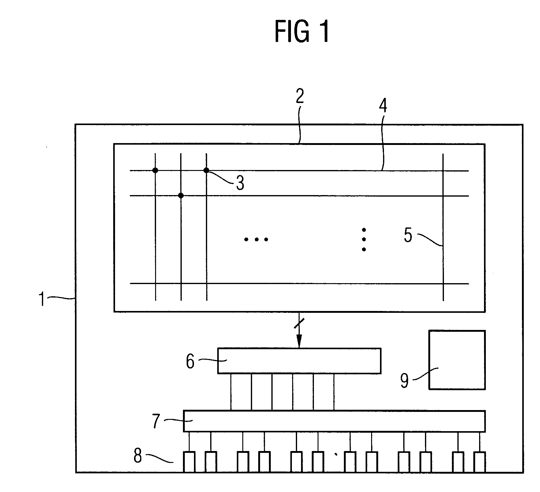
[0023]FIG. 1 shows a memory device 1 including a memory array 2. The memory array comprises memory cells 3 arranged on wordlines 4 and bitlines 5. For example the memory cells can be DRAM memory cells, SRAM cells and the like.

[0024] The memory device 1 is designed e.g. as a Double Data Rate memory device from which data can be read out in a burst access which means that by applying an address to the memory array 2, a number of data bits is internally provided for outputting in groups of a number of parallel data bits in a number of successive cycles.

[0025] This is e.g. achieved by simultaneously addressing a plurality of memory areas (banks etc.) which provide data to be read out from the addressed memory cells 3 and forward the read-out data to a pre-fetch buffer 6 wherein the data is latched until it is forwarded to output via a number of output ports 8. The pre-fetch is performed by the pre-fetch read unit 9.

[0026] In conventional memory devices, the number of pre-fetched data...


PUM


Abstract

The present invention relates to an integrated memory device including: memory cells arranged at wordlines and bitlines, wherein the memory cells are addressable in sets of 2n bit, wherein n is an integer, a pre-fetch read unit to pre-fetch an addressed set of 2n data bit in parallel from the addressed memory area, buffer memory to buffer the number of pre-fetched data bits; a number m of output ports to output the data bits buffered in the buffer memory; an output controller for controlling the outputting of the data bits buffered in the buffer memory to the number m of output ports in groups of m bits in one or a plurality of successive cycles, characterized in that the number m of output ports is different to any of the possible numbers 2n of the sets of addressable memory cells.

Description

BACKGROUND OF THE INVENTION [0001] 1. Field of the Invention [0002] The present invention relates to an integrated memory device having a number of memory cells which are addressable by an address and wherein data is prefetched in sets of 2n bit. The present invention further relates to a memory module having a plurality of memory devices. [0003] 2. Description of the Related Art [0004] In DDR (Double Data Rate) memory devices, data in memory cells is conventionally addressable by an address in sets of 2n bit or multiples thereof. Each set of bits addressed by the address is pre-fetched in a pre-fetch buffer when retrieving data from the memory cells. Once the data from the addressed memory area is held in the pre-fetch buffer, the data is usually output in a sequence of successive cycles via output ports, in a so-called data burst. The data is output according to the Double Data Rate technology with rising and falling edges of a clock signal and the number of output cycles depends ...

Claims


Application Information

Patent Timeline
Patent Type & Authority Applications(United States)
IPC IPC(8): G06F13/00
CPCG06F12/0862G06F2212/6022
Inventor SICHERT, CHRISTIANRUCKERBAUER, HERMANNSAVIGNAC, DOMINIQUEGREGORIUS, PETERWALLNER, PAUL
Owner INFINEON TECH AG
Why Eureka
Try Eureka