Differential clock transmission apparatus, differential clock sending apparatus, differential clock receiving apparatus and differential clock transmission method
- Summary
- Abstract
- Description
- Claims
- Application Information
AI Technical Summary
Benefits of technology
Problems solved by technology
Method used
Image


Examples
first embodiment
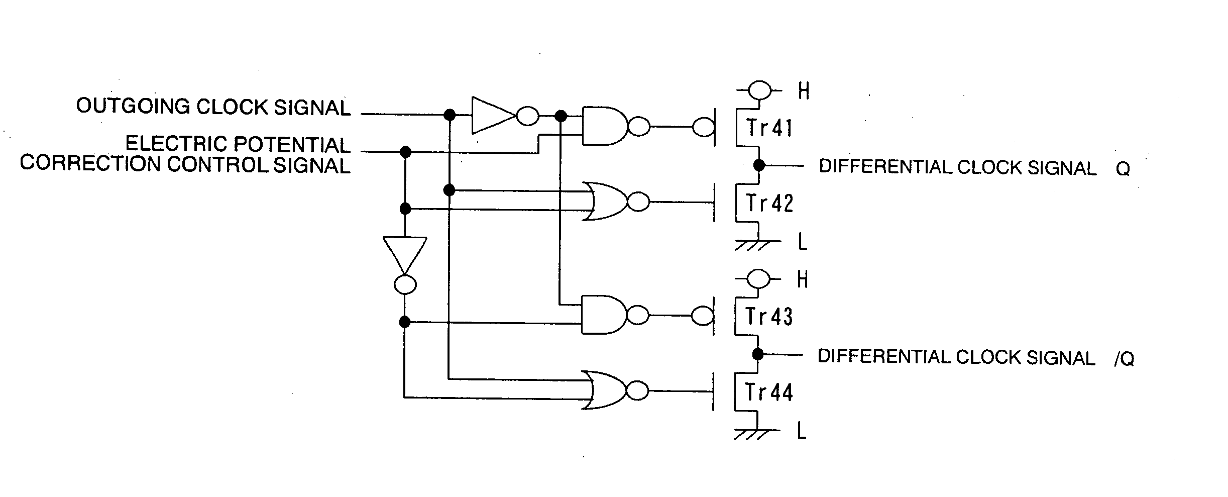
[0038] In this embodiment, the signal sending side is adapted to correct electric potentials. FIG. 1 is a schematic block diagram of the first embodiment of differential clock transmission apparatus according to the present invention, showing the configuration thereof. In FIG. 1, the components that are identical with or equivalent to the corresponding ones of FIG. 12 are denoted respectively by the same reference symbols and will not be described here any further. By comparing with the differential clock transmission apparatus of FIG. 12, it will be seen that the differential clock transmission apparatus of FIG. 1 comprises a clock sending side LSI 1 in place of the clock sending side LSI 901 of FIG. 12 and a clock receiving side LSI 2 in place of the clock receiving side LSI 902 of FIG. 12. By comparing with the clock sending side LSI 901 of FIG. 12, it will also be seen that the clock sending side LSI 1 of FIG. 1 additionally has an electric potential correcting section 14 and al...
second embodiment
[0046] In this embodiment, the electric potential correcting operation is conducted by the receiving side to obtain advantages similar to those of the first embodiment. FIG. 7 is a schematic block diagram of the second embodiment of differential clock transmission apparatus according to the invention, showing the configuration thereof. In FIG. 7, the components that are identical with or equivalent to the corresponding ones of FIG. 1 are denoted respectively by the same reference symbols and will not be described here any further. By comparing with the differential clock transmission apparatus of FIG. 1, it will be seen that the differential clock transmission apparatus of FIG. 7 comprises a clock sending side LSI 101 in place of the clock sending side LSI 1 and a clock receiving side LSI 102 in place of the clock receiving side LSI 2.
[0047] By comparing with the clock sending side LSI 1, it will be seen that the clock sending side LSI 101 of FIG. 7 has a sending control section 11...
third embodiment
[0048] In this embodiment, while the electric potential correcting operation is conducted by the sending side, the sending side is so configured as to have both the function of converting an outgoing clock signal into a pair of differential clock signals and the electric potential correcting function to obtain advantages similar to those of the above described embodiments. FIG. 8 is a schematic block diagram of the third embodiment of differential clock transmission apparatus according to the invention, showing the configuration thereof. In FIG. 8, the components that are identical with or equivalent to the corresponding ones of FIG. 1 are denoted respectively by the same reference symbols and will not be described here any further. By comparing with the differential clock transmission apparatus of FIG. 1, it will be seen that the differential clock transmission apparatus of FIG. 8 comprises a clock sending side LSI 201 in place of the clock sending side LSI 1 and a clock receiving ...
PUM
 Abstract
Description
Claims
Application Information