Vertical-alignment liquid crystal display device

a liquid crystal display and active matrix technology, applied in non-linear optics, instruments, optics, etc., can solve problems such as uniform display states of respective pixels, and achieve the effect of reducing disturbance in alignment between pixels and excellent quality

Inactive Publication Date: 2006-06-01
CASIO COMPUTER CO LTD
View PDF55 Cites 29 Cited by
  • Summary
  • Abstract
  • Description
  • Claims
  • Application Information

AI Technical Summary

Benefits of technology

[0009] An object of the present invention is to provide a vertical-alignment active matrix liquid crystal display device

Problems solved by technology

However, conventional vertical-alignment active matrix liquid crystal display devices have a problem that the tilted-alignment state of liquid

Method used


Image

  • Vertical-alignment liquid crystal display device
  • Vertical-alignment liquid crystal display device
  • Vertical-alignment liquid crystal display device

Examples


first embodiment

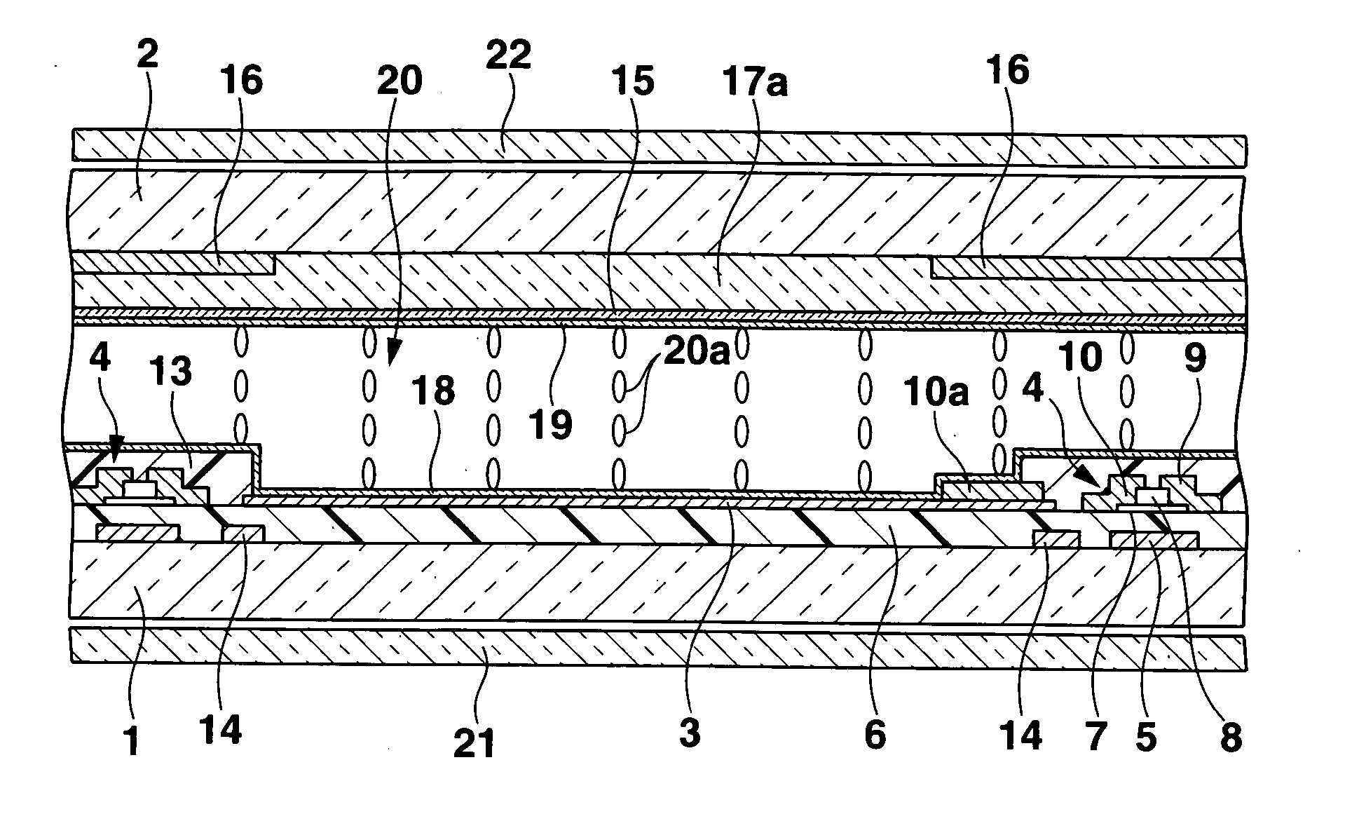
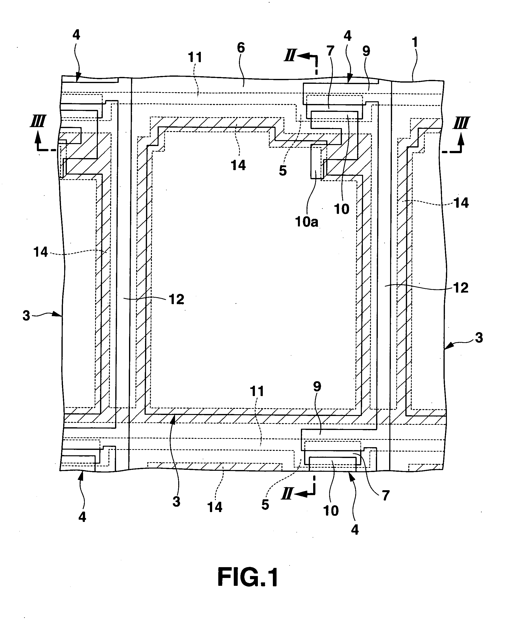
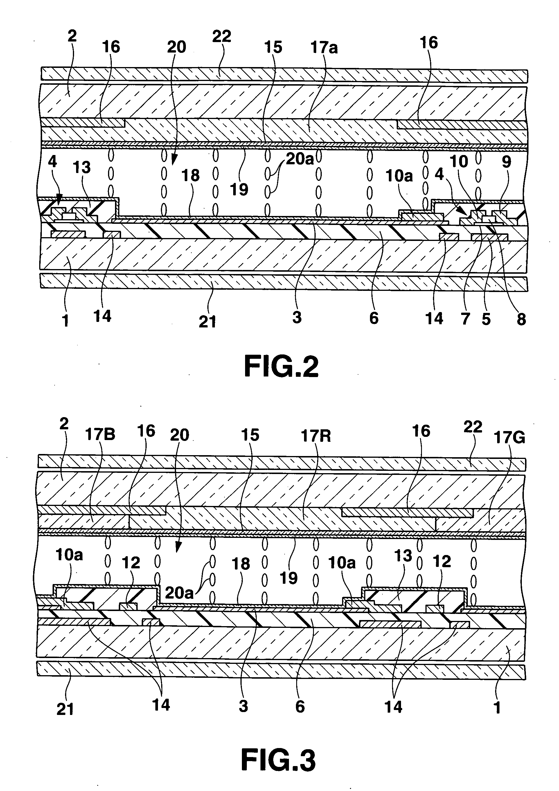
[0040] FIGS. 1 to 5 shows the first embodiment of the present invention. FIG. 1 is a plan view of one pixel part in one substrate of a liquid crystal display device. FIGS. 2 and 3 are cross-sectional views showing the liquid crystal display device, cut along the lines II-II and III-III in FIG. 1.

[0041] This liquid crystal display device is a vertical-alignment active matrix liquid crystal display device in which TFTs are active elements. As shown in FIGS. 1 to 3, the liquid crystal display device has a pair of transparent substrates 1 and 2 opposed to each other with a predetermined gap maintained therebetween; plural transparent electrodes 3 which are provided on the inner surface of the substrate 1, of mutually-opposing inner surfaces of the paired substrates 1 and 2, and are arrayed in a matrix along row and column directions; plural TFTs 4 provided on the inner surface of the substrate 1, respectively near and corresponding to the plural pixel electrodes 3, and connected respec...

second embodiment

[0077]FIG. 6 shows the second embodiment of the present invention. FIG. 6 is a plan view showing of one pixel part in one substrate (TFT substrate) of the liquid crystal display device.

[0078] In the liquid crystal display device according to this second embodiment, auxiliary electrodes formed on the TFT substrate have a different shape from that of the auxiliary electrodes in the first embodiment. The other features of the structure are the same as those of the liquid crystal display device according to the first embodiment. Therefore, the same members as those in the first embodiment are denoted at the same reference symbols, and detailed descriptions thereof will be omitted herefrom.

[0079] That is, the auxiliary electrodes 14 each are made of a conductive film formed in a frame-like shape surrounding the whole periphery of a pixel electrode 3 on the substrate surface of the TFT substrate 1, like in the first embodiment. This frame-like conductive film is made of a metal film, tr...

third embodiment

[0083]FIG. 7 shows the third embodiment of the present invention. FIG. 7 is a plan view showing one pixel part in one substrate (TFT substrate) of the liquid crystal display device.

[0084] In the liquid crystal display device according to this third embodiment, auxiliary electrodes formed on the TFT substrate have a different shape from that of the auxiliary electrodes in the first embodiment. The other features of the structure are the same as those of the liquid crystal display device according to the first embodiment. Therefore, the same members as those in the first embodiment are denoted at the same reference symbols, and detailed descriptions thereof will be omitted herefrom.

[0085] That is, the auxiliary electrodes 14 each are made of a conductive film formed in a frame-like shape surrounding the whole periphery of a pixel electrode 3 on the substrate surface of the TFT substrate 1, like in the first embodiment. Edge portions of the auxiliary electrode 14 are formed to be suc...


PUM


Abstract

A vertical-alignment liquid crystal display device includes: one substrate on which plural pixel electrodes and thin film transistors (TFTs) corresponding to the pixels, scanning signal lines for supplying gate electrodes of these TFTs with a gate signal, and data signals lines for supplying drain electrodes of the TFTs with data signals are provided; an opposing substrate on which an opposing electrode opposed to the pixel electrodes is provided; vertical-alignment films covering surfaces of the respective substrates where electrodes are formed; and a liquid crystal layer sealed between these substrates and having a negative dielectric constant. On the inner surface of the one substrate, auxiliary electrodes to generate electric fields of a predetermined value between the auxiliary electrodes and the opposing electrode provided on the inner surface of the other substrate are provided respectively corresponding to those portions around the plural pixel electrodes that are close to at least the TFTs.

Description

BACKGROUND OF THE INVENTION [0001] 1. Field of the Invention [0002] The present invention relates to a vertical alignment active matrix liquid crystal display device in which thin film transistors (hereinafter referred to as TFTs) are active elements. [0003] 2. Description of the Related Art [0004] A vertical-alignment liquid crystal display device has: a pair of substrates which are opposed to each other with a predetermined gap maintained between each other, plural electrodes which are provided on each of opposed inner surfaces of the paired substrates, to form plural pixels arrayed in a matrix on regions opposed to each other; vertical-alignment films provided respectively on the inner surfaces of the paired substrates covering the electrodes; and a liquid crystal layer which is sealed in the gap between the paired substrates and has negative dielectric anisotropy. [0005] In this vertical-alignment liquid crystal display device, the alignment state of liquid crystal is changed fr...

Claims


Application Information

Patent Timeline
IPC IPC(8): G02F1/1343G02F1/1337
CPCG02F1/1343G02F1/1393G02F1/1337
Inventor MIZUSAKO, RYOTAYAMAGUCHI, MINORU
Owner CASIO COMPUTER CO LTD
Why Eureka
Try Eureka