Imaging device and an imaging method

a technology of imaging device and image, which is applied in the direction of radio frequency controlled devices, instruments, television systems, etc., can solve the problems of only detecting one color in individual pixels, limiting achromatism, and being unable to completely separate light, etc., to achieve clear luminance information or monochrome images, good color reproducibility, and high color reproducibility and color resolution

Active Publication Date: 2006-06-01
PANASONIC CORP
View PDF26 Cites 30 Cited by
  • Summary
  • Abstract
  • Description
  • Claims
  • Application Information

AI Technical Summary

Benefits of technology

[0026] With this configuration, clear color images with good color reproducibility can be obtained, and at the same time clear luminance information or monochrome images can be obtained. As a result, for example, color images with high color reproducibility and color resolution can be provided in the daytime; sharp monochrome images can be obtained eve...

Problems solved by technology

Of course, it is actually impossible to separate light completely.
However, in conventional visible light and near infrared light imaging devices such as the one described in the above-mentioned Japanese Patent Laid-Open Application No. 2002-142228, individual pixels can only detect one color (limited wavelength region).
However, there is a limit to achromatism.
It is difficult to make a perfect achromatic optical system for a very wide range of wavelengths from the visible light region to the near infrared light region (from 400 nm to 1000 nm).
Even if it could be made, such optical system would be very expensive, so that it is difficult to use in current common industrie...

Method used


Image

  • Imaging device and an imaging method
  • Imaging device and an imaging method
  • Imaging device and an imaging method

Examples


first embodiment

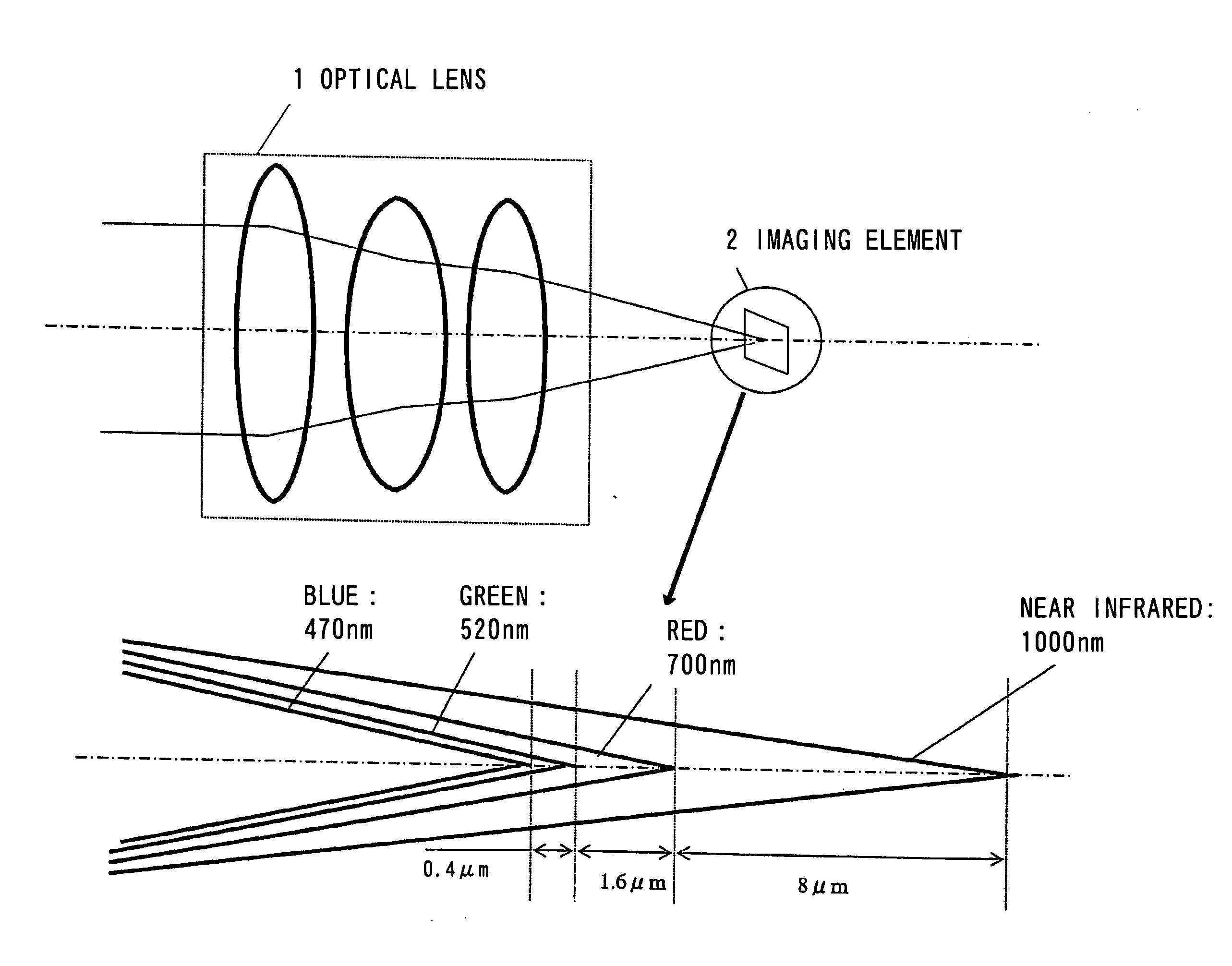
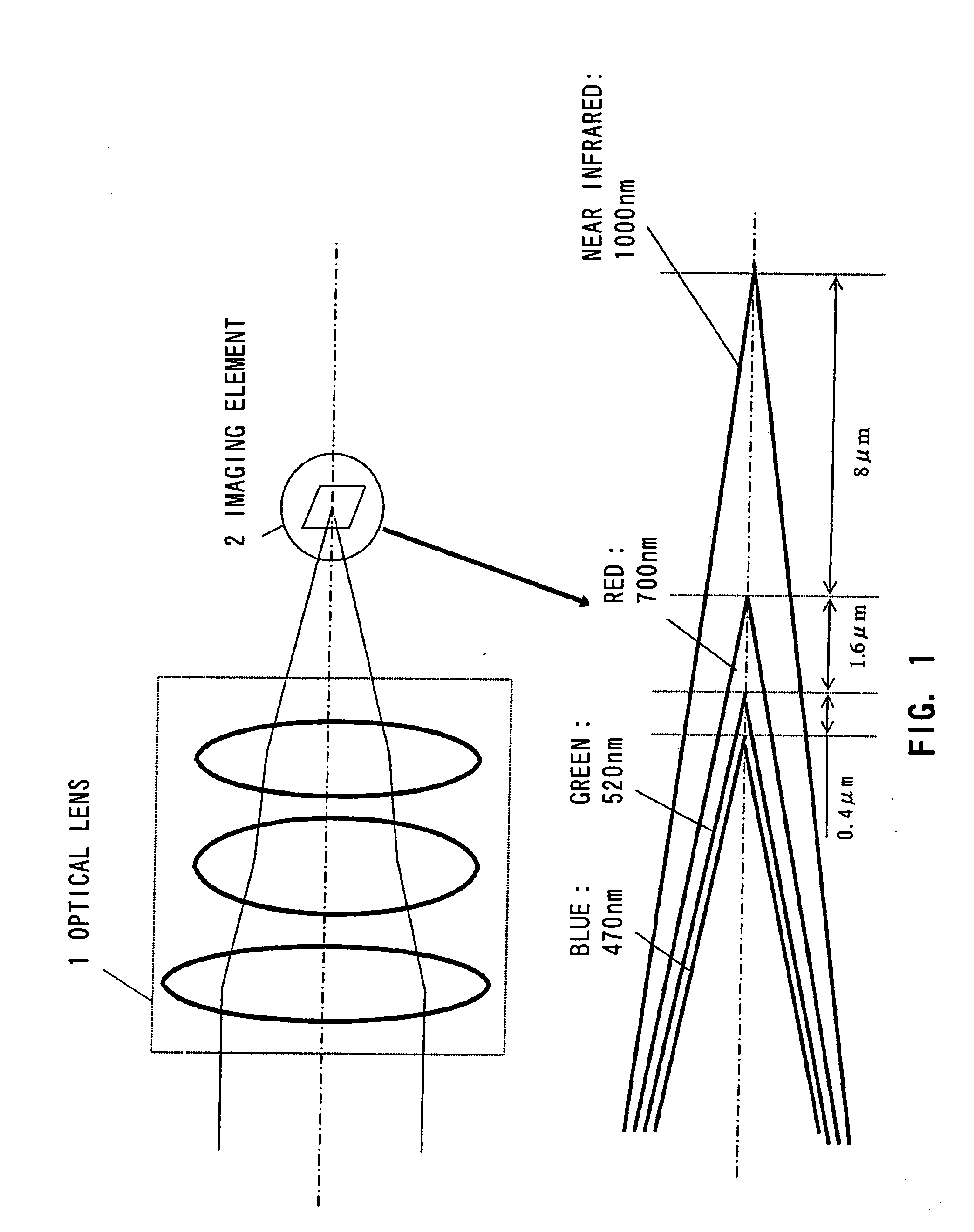
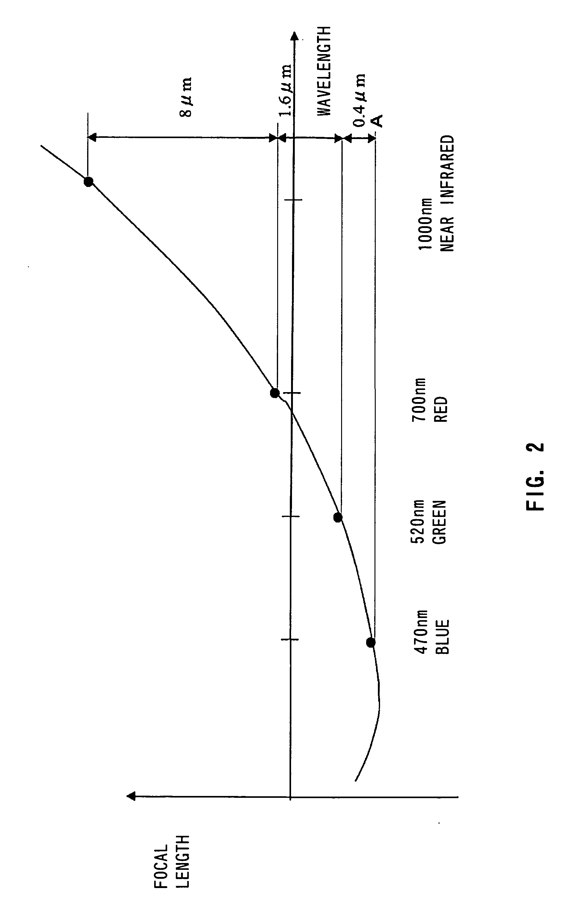
[0041] As shown in FIG. 1, a visible light and near infrared light imaging device related to the invention has an optical lens 1. The optical lens 1 is an optical system whose focal length is variable according to wavelengths, and makes three components of visible light and near infrared light in different wavelength regions form images at different locations according to their wavelengths. The optical lens 1 condenses light from an external subject and forms an image on an imaging element 2. In the lower part of FIG. 1, light pencils from the optical lens 1 are shown separately by different wavelengths. The optical lens 1 forms images at different locations according to wavelengths as described above. This is shown more specifically in FIG. 2. For example, if blue of 470 nm is a focal-point reference A, the focal length of green of 520 nm is 0.4 μm longer than the reference A. Similarly, the focal length of red of 700 nm is 2 μm longer than the reference A, and the focal length of ...

second embodiment

[0057] Next, FIG. 8 shows a configuration of an imaging element related to a second embodiment, and FIG. 9 is an equivalent circuit schematic of an imaging element related to the second embodiment. In the imaging element shown in FIG. 8, a visible light detection section and near infrared light detection section are placed in one pixel. The figure shows one pixel, which comprises a detection section to separate and detect three components of visible light and near infrared light in different wavelength regions, four components in total. In other words, four current detectors 23, 24, 25, and 26 arranged in one pixel detect B, G, and R of visible light and near infrared light. As shown in FIG. 8, an n-type doped region 19 of an n-type semiconductor is formed on a p-type semiconductor substrate 9. Similarly, a p-type doped region 20 is formed thereon. Moreover, an n-type doped region 21 is formed thereon. Furthermore, a p-type doped region 22 is formed thereon. In this way, a four-laye...


PUM


Abstract

An optical lens 1 makes three components of visible light and near infrared light in different wavelength regions severally form images at different locations according to their wavelengths. An imaging element 2 has a plurality of pixels, which include pixels having a visible light detection section 6 and pixels having a near infrared light detection section 8. The visible light detection section 6 has three detectors 3, 4, and 5 which detect three components of visible light which form images at locations of different depths in the same pixel according to their wavelengths. The near infrared light detection section 8 has a near infrared light detector 7 which detects near infrared light which forms an image at a location of a depth different from the depths at which the three components of visible light form images. Clear color images with good color reproducibility are obtained by the visible light detection section 6, and at the same time clear luminance information or monochrome images are obtained by the near infrared light detection section 8.

Description

TECHNICAL FIELD [0001] The present invention relates to an imaging device and imaging method for detecting and receiving three components of visible light and near infrared light in different wavelength regions and for imaging pictures of both visible light and near infrared light. BACKGROUND ART [0002] Conventional visible light and near infrared light imaging devices have a configuration in which each of pixels can detect one of three colors of different wavelengths in visible light and near infrared light and such pixels are arranged in a mixed manner in the same imaging element, for example a CCD or CMOS imaging element (e.g. see FIG. 2 of Japanese Patent Laid-Open Application No. 2002-142228). For example, as shown in FIG. 10, Mg (magenta) color detectors 81, Ye (yellow) color detectors 82, Cy (cyan) color detectors 83, and near infrared light detectors 84 are arranged on an imaging element like amosaic so that the combination repeats lengthwise and crosswise. Here, one detecto...

Claims


Application Information

Patent Timeline
IPC IPC(8): G06K7/10G02B3/00H01L27/14G06T1/00H01L27/146H01L31/10H01L31/101H04N1/028H04N5/335H04N5/369H04N9/04H04N9/07
CPCH01L27/14645H01L31/101H04N5/332H04N9/045H04N2209/047H04N23/11H04N25/131H04N25/17
Inventor OKADA, TSUYOSHIISHII, HIROFUMIMIZUSAWA, KAZUFUMI
Owner PANASONIC CORP
Why Eureka
Try Eureka