Semiconductor device and method of manufacturing the same

Inactive Publication Date: 2006-06-01
NEC ELECTRONICS CORP
View PDF1 Cites 5 Cited by
  • Summary
  • Abstract
  • Description
  • Claims
  • Application Information

AI Technical Summary

Benefits of technology

[0030] Thus, according to the invention, the semiconductor device which includes the barrier metal having the high adhesiveness and diffusion b

Problems solved by technology

In the barrier metal layer 210, it is difficult that compatibility between the diffusion barrier properties and the adhesiveness.
However, because the PVD method has a worse step coverage, a thickness of a side wall portion is decreased when compared with the thickness of a bottom portion in the interconnect trench or the via hole.
However, in the PVD method, it is difficult that the thin film is conformaly formed, so that another technique is required in order to form the barrier metal having the thickness of not more than 10 nm.
However, in the ALD method, since the film formation is performed by the saturat

Method used


Image

  • Semiconductor device and method of manufacturing the same
  • Semiconductor device and method of manufacturing the same
  • Semiconductor device and method of manufacturing the same

Examples


Example

[0043] The invention will be now described herein with reference to illustrative embodiments. Those skilled in the art will recognize that many alternative embodiments can be accomplished using the teachings of the present invention and that the invention is not limited to the embodiments illustrated for explanatory purposed.

[0044] Embodiments of the invention will be described in detail with reference to the drawings.

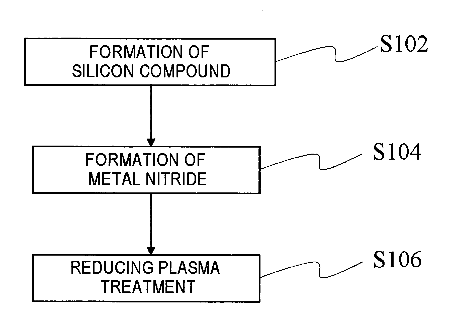
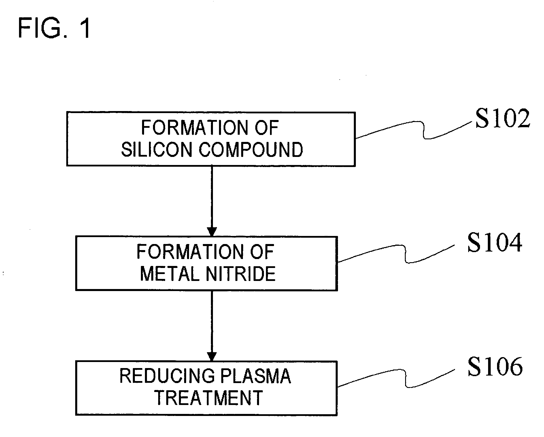
[0045]FIG. 1 is a flowchart showing a main part of a method of manufacturing a semiconductor device according to an embodiment of the invention.

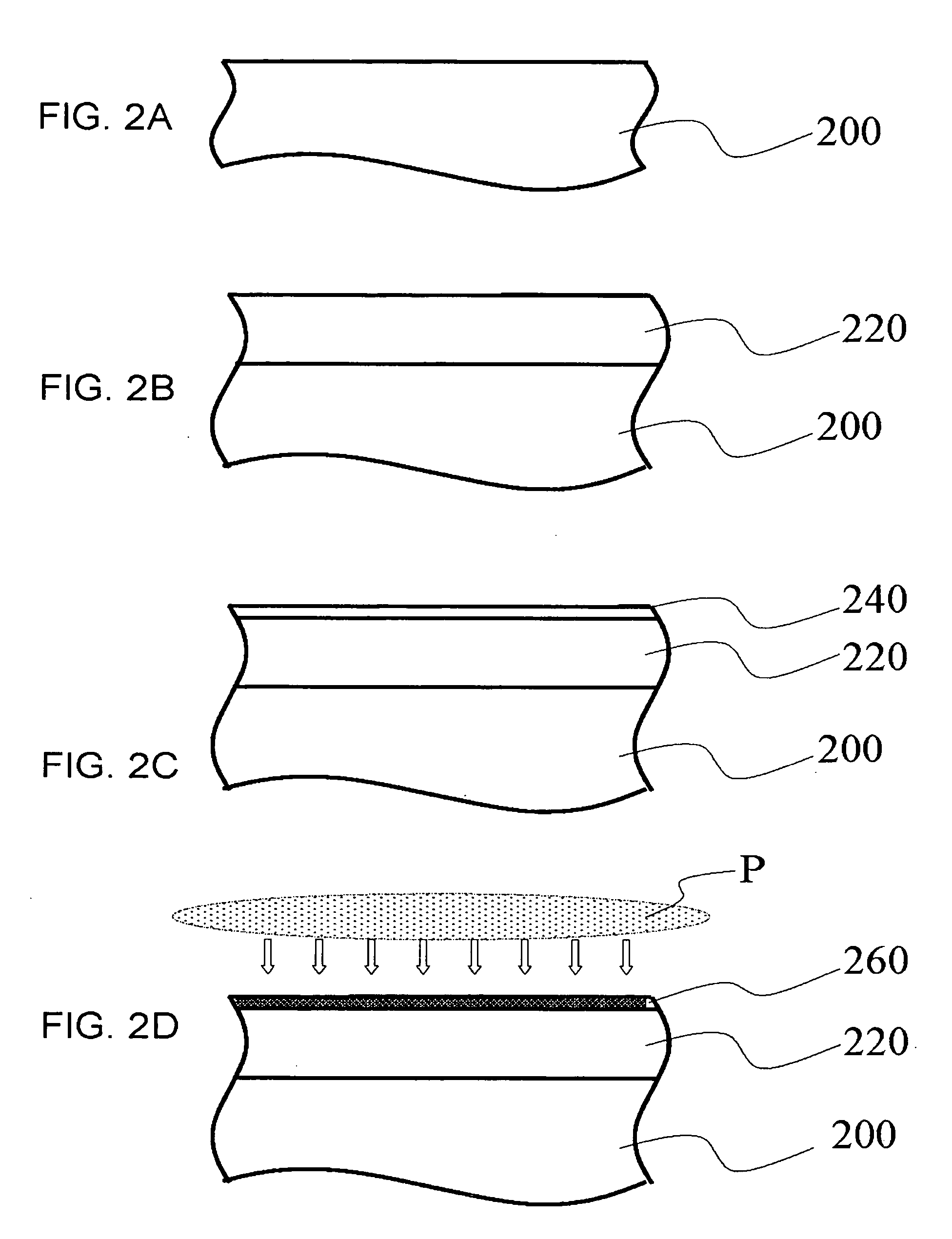
[0046]FIGS. 2A to 2D is a process cross-sectional view showing the main part of the method of manufacturing the semiconductor device according to the embodiment.

[0047] In the embodiment, as shown in FIGS. 2A and 2B, a silicon compound 220 is formed on the base substance 200 (Step S102). As described later, a semiconductor wafer on which elements such as a transistor are formed is used as the base substance 200. A compound o...


PUM


Abstract

An object of the invention is to provide a semiconductor device which includes a barrier metal having high adhesiveness and diffusion barrier properties and a method of manufacturing the semiconductor device. The invention provides a semiconductor device manufacturing method including forming a first layer made of a material containing silicon on a base substance; forming a second layer containing metal and nitrogen on the first layer; and exposing the second layer to active species obtained from plasma in an atmosphere including reducing gas.

Description

[0001] This application is based on Japanese Patent application NO. 2004-343443, the content of which is incorporated hereinto by reference. BACKGROUND [0002] 1. Technical Field [0003] The present invention relates to a semiconductor device and a method of manufacturing the same, particularly to the semiconductor device which has an insulating interlayer and uses a Cu (copper) interconnect and the method of manufacturing the same. [0004] 2. Related Art [0005] In recent semiconductor devices represented by a 65-nm node generation, delay of signal propagation in an interconnect is known as a rate-controlling factor in device operation. A delay constant at the interconnect is expressed by a product of interconnect resistance and capacitance among the interconnect. Therefore, in order to increase speed of the device operation by decreasing the interconnect resistance and capacitance among the interconnect, a material (hereinafter referred to as “low dielectric constant material”) having...

Claims


Application Information

Patent Timeline
IPC IPC(8): H01L21/20H01L21/36
CPCH01L21/318H01L21/3185H01L21/76846H01L21/76855H01L2924/0002H01L21/76862H01L2924/00H01L21/02123H01L21/022H01L21/02175H01L21/02337H01L21/0234
Inventor FURUYA, AKIRAOTSUKA, NOBUYUKIOKAMURA, HIROSHIOGAWA, SHINICHI
Owner NEC ELECTRONICS CORP
Why Eureka
Try Eureka