Method of modifying a surface of an insulator

a technology of insulator and surface, applied in the field of surface modification, can solve the problems of excessive elongation of process time, inability to easily improve productivity, and limited application method of electric beam of the foregoing type, so as to achieve the effect of reducing time required to complete the process, reducing labor intensity, and efficient subjecting to the surface modification

Inactive Publication Date: 2001-06-21
SONY CORP
View PDF0 Cites 4 Cited by
  • Summary
  • Abstract
  • Description
  • Claims
  • Application Information

AI Technical Summary

Benefits of technology

0010] According to the foregoing method for surface modification of an insulator arranged to apply the pulse-shape voltage, a fact that the insulator is brought into an electrical non-equilibrium, that is, a charge-up state, can be prevented even if the insulator is continuously irradiated with electron beams. Therefore, even the insulator can continuously and effectively be irradiated with the electron beams. As a result, time required to complete the process can be shortened, causing the productivity to be improved.
0011] According to the present invention, surface modification using the electron-beam applying method can be applied to plastic, which is the insulator. Therefore, the plastic can efficiently be subjected to the surface modification. That is, according to the present invention, plastic can be subjected to surface modification using electron-beam applying method so that physical and chemical characteristics are improved which include hardness, elasto-plasticity, electric conductivity, lubricity, durability, moisture resistance, corrosion resistance, wettability and gas permeability. Therefore, the present invention enables a variety of materials which have been made of metal or glass into low-cost plastic. Hence it follows that a significant industrial advantage can be obtained.

Problems solved by technology

The electron-beam applying method of the foregoing type, however, has been limited to a case in which the work 101 which must be processed is made of a material, such as metal, having conductivity.
Hence it follows that the time to complete the process is elongated excessively when the electron-beam applying method is applied to the insulator.
As a result, there arises a problem in that the productivity cannot easily be improved.
When the conventional electron-beam applying method is applied to the insulator, such as plastic, there arises a problem in that the work 101 which must be processed is melted or deformed owing to the heat generated by the electron beam.

Method used


Image

  • Method of modifying a surface of an insulator
  • Method of modifying a surface of an insulator
  • Method of modifying a surface of an insulator

Examples


second example

[0062] In this example, a plastic substrate obtained by molding polyimide resin was employed as the work 11 which must be processed. Then, the surface modification was performed similarly to the first example. Then, wettability of the plastic substrate subjected to the surface modification with respect to water was measured. The measurement was performed by using a contact angle meter (CA-D contact angle meter manufactured by Kyowa Interface). As a result, the contact angle between the plastic substrate which was not subjected to the surface modification and water was 106.degree.. On the other hand, the angle of contact between the plastic substrate subjected to the surface modification and water was 50.degree.. Therefore, the method for surface modification according to the present invention was able to modify the surface of the plastic substrate and change the wettability.

[0063] Then, electric resistance of the surface of the plastic substrate was measured. Thus, the electric resi...

third example

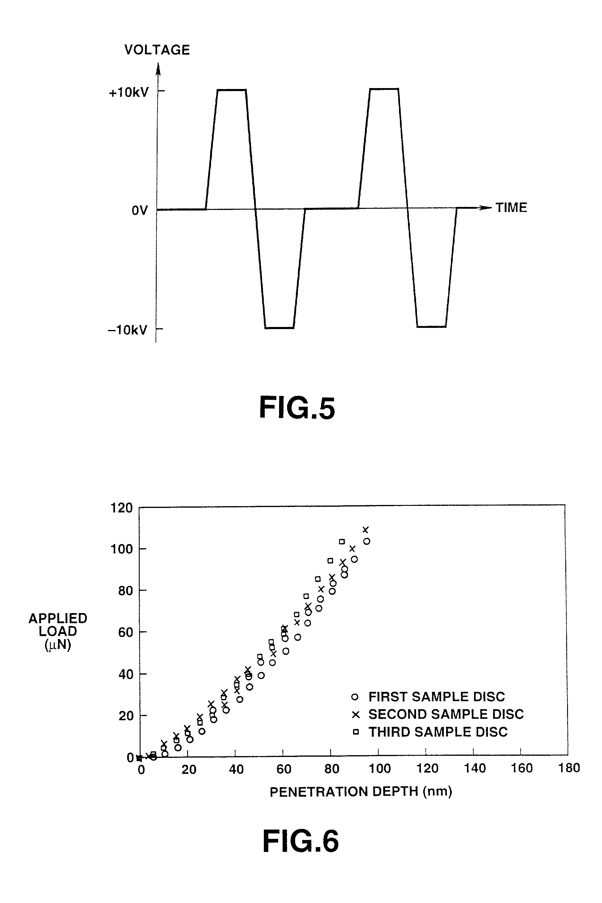
[0064] In this example, a plastic substrate obtained by molding amorphous polyolefine (APO) was employed as the work 11 which must be processed. Then, the surface modification was performed similarly to the first example. In the third example, the pulse-shape voltage which was applied to the plastic substrate had a waveform similarly to the first example and as shown in FIG. 5 such that the positive pulse-shape voltage and the negative pulse-shape voltage alternately appeared.

[0065] In the third example, three sample discs were manufactured under the following surface modification conditions. The other conditions were the same as those in the first example.

[0066] Surface Modification Conditions

[0067] Pulse Peak Voltage: +10 kV, -10 kV

[0068] Interval between Pulses: 10 msec (10 kHz)

[0069] Process Duration: 10 minutes

[0070] Each of the manufactured sample discs was subjected to the nano-indentation test similarly to the first example. Results of the measurement were shown in FIG. 6. I...


PUM

PropertyMeasurementUnit
voltagesaaaaaaaaaa
pressureaaaaaaaaaa
contact angleaaaaaaaaaa

Abstract

When an insulator is irradiated with an electron beam, a pulse-shape voltage is applied to the insulator from a pulse power source. As a result, a charge-up state of the insulator can be prevented. If an object which must be subjected to surface modification is an insulator, the object can effectively be irradiated with the electron beam to perform the surface modification.

Description

[0001] 1. Field of the Invention[0002] The present invention relates to a method for surface modification by irradiating an insulator with an electron beam to modify the surface of the insulator.[0003] 2. Description of the Related Art[0004] A method has been employed which subjects a work which must be processed to surface modification to modify a variety of physical and chemical characteristics including hardness, elasto-plasticity, electric conductivity, lubricity, durability, moisture resistance, corrosion resistance, wettability and gas permeability. As the foregoing method, a method (hereinafter called an "electron-beam applying method") has been known with which a work which must be processed is irradiated with an electron beam to modify the surface of the work.[0005] The electron-beam applying method is, as shown in FIG. 1, performed such that a work 101 which must be processed and which is secured to a holder 100 in a vacuum chamber is irradiated with an electron beam 103 e...

Claims


Application Information

Patent Timeline
Patent Type & Authority Applications(United States)
IPC IPC(8): H01J37/317B29C35/08B29C59/16C03C23/00H01L21/312
CPCB29C59/16B29C2035/0877C03C23/004
Inventor TONOSAKI, MINEHIROUEDA, MITSUNORIKOBAYASHI, MASATOOKITA, HIROYUKI
Owner SONY CORP
Why Eureka
Try Eureka