

Formation of deep trench airgaps and related applications
a technology of air gap and deep trench, applied in the field of trench formation, can solve the problems of inability to meet the requirements of the active device area, the collector substrate capacitance is a significant contributor to the total switching delay, and the process limitations of many methods are not very scalable, so as to reduce the perimeter capacitance of the parasitic collector substrate, reduce the width of the deep trench, and reduce the total device area
- Summary
- Abstract
- Description
- Claims
- Application Information
AI Technical Summary
Benefits of technology
Problems solved by technology
Method used
Image

Examples
Embodiment Construction
[0039] The following description and examples illustrate a preferred embodiment of the present invention in detail. Those of skill in the art will recognize that there are numerous variations and modifications of this invention that are encompassed by its scope. Accordingly, the description of a preferred embodiment should not be deemed to limit the scope of the present invention.
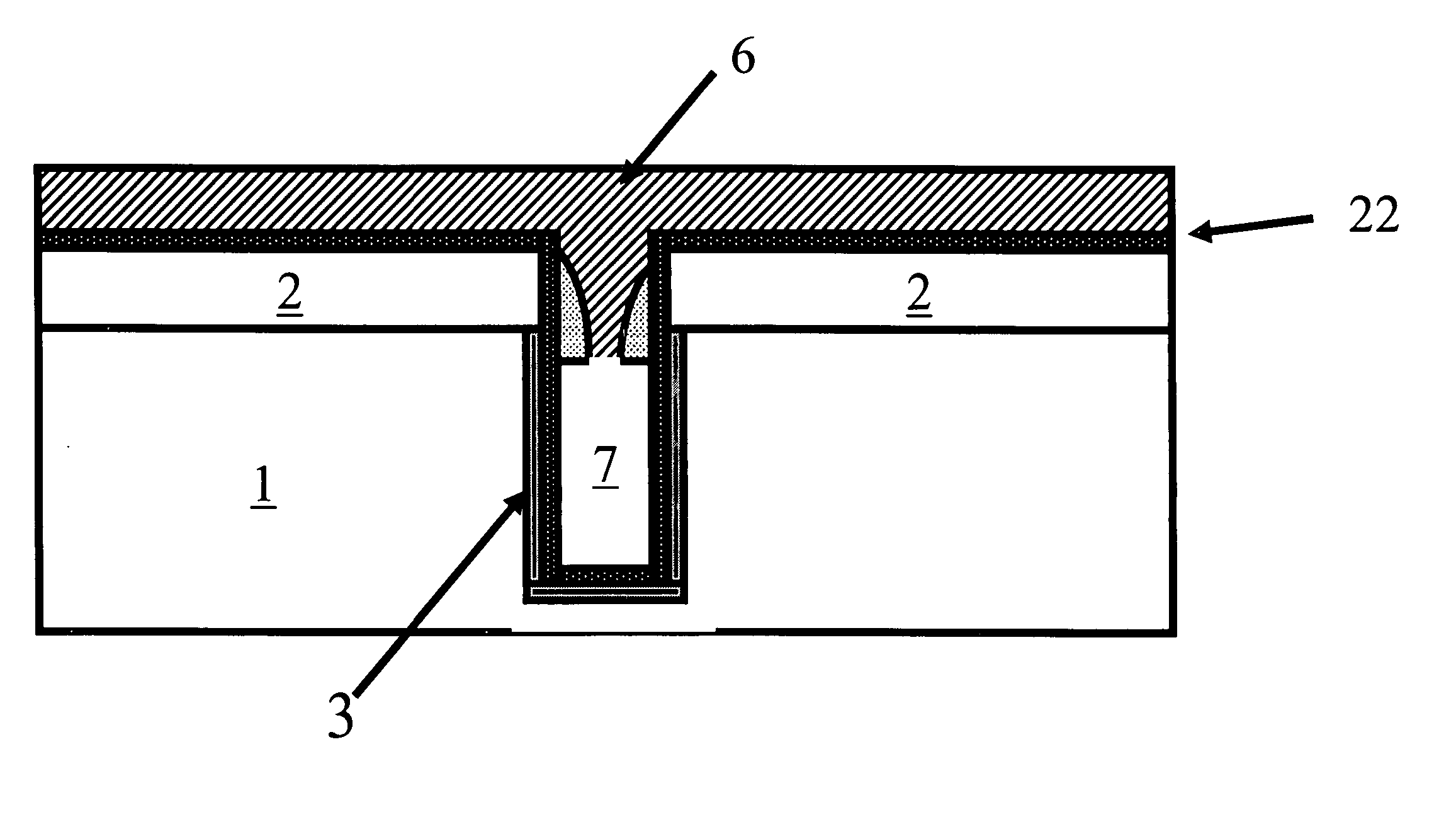
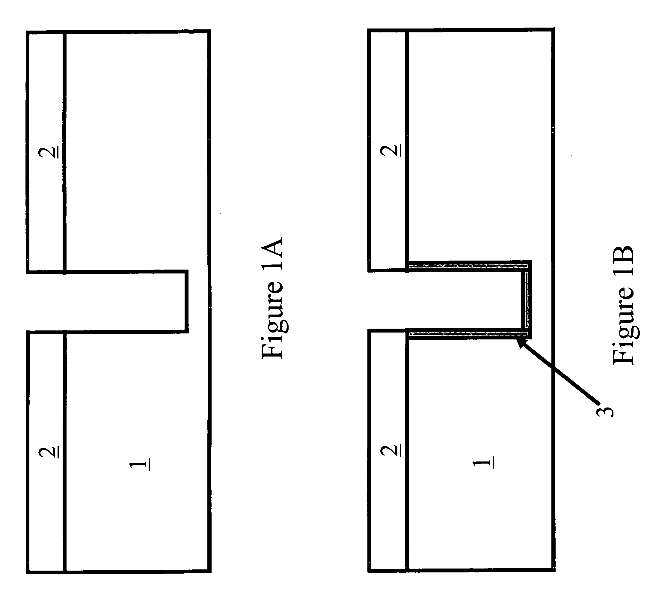
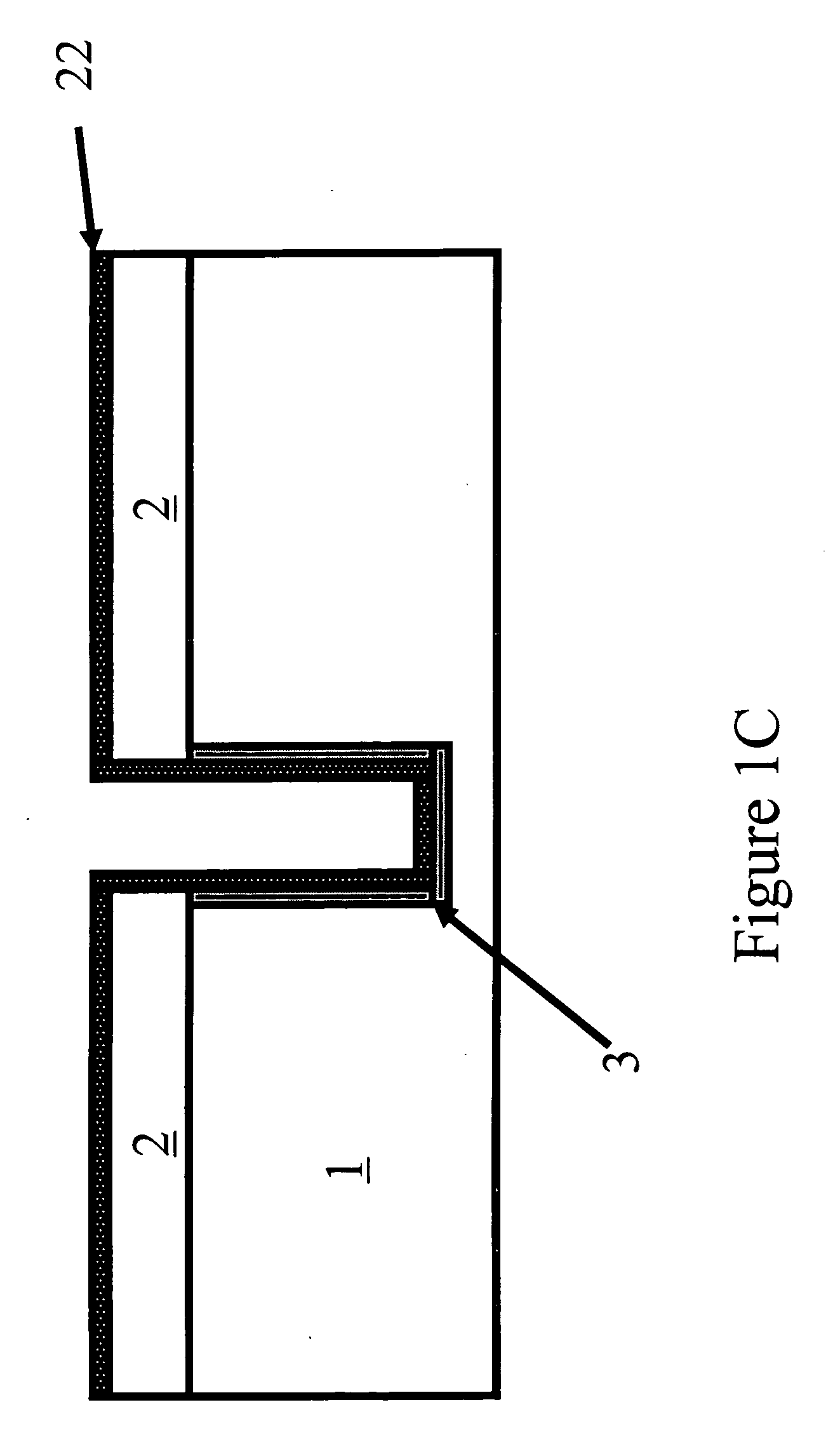
[0040] The term “sacrificial,” as used herein, is a broad term and is used in its ordinary sense, including, without limitation, a material or a layer that is deposited temporarily, and that is not supposed to remain, at least totally, in the final device, or a material or layer that is destined to be removed, at least partially, during the process of fabricating a device.
[0041] The term “spacer,” as used herein, is a broad term and is used in its ordinary sense, including, without limitation, a material or layer that is deposited on a side wall of a trench, hole, via, or other structure that is partially...
PUM
 Abstract
Description
Claims
Application Information