
Delay locked loop for use in semiconductor memory device and method thereof

Active Publication Date: 2006-06-22
SK HYNIX INC
View PDF5 Cites 11 Cited by
  • Summary
  • Abstract
  • Description
  • Claims
  • Application Information

AI Technical Summary

Benefits of technology

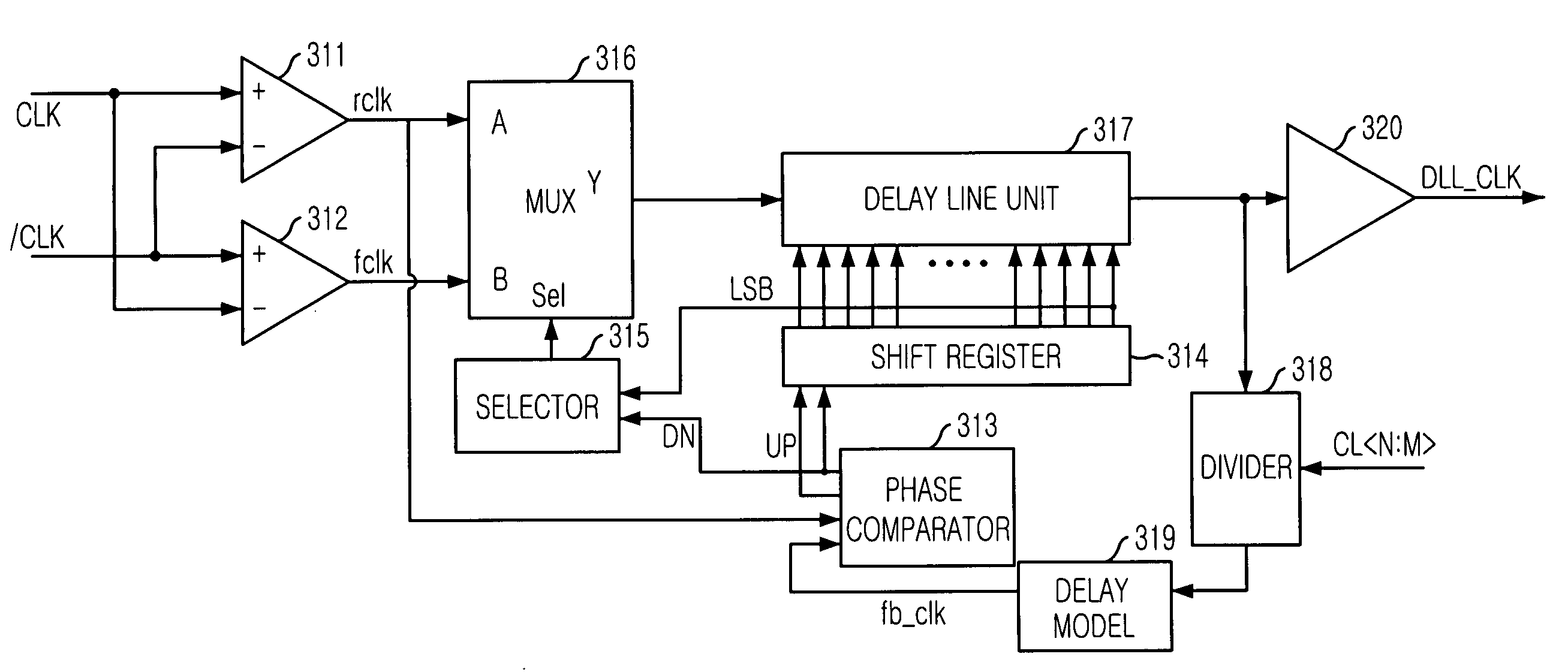
[0022] It is, therefore, an object of the present invention to provide a delay locked loop (DLL), which is stably operated at a high operational frequency, for reducing a power consumption and a circuit size.

Problems solved by technology

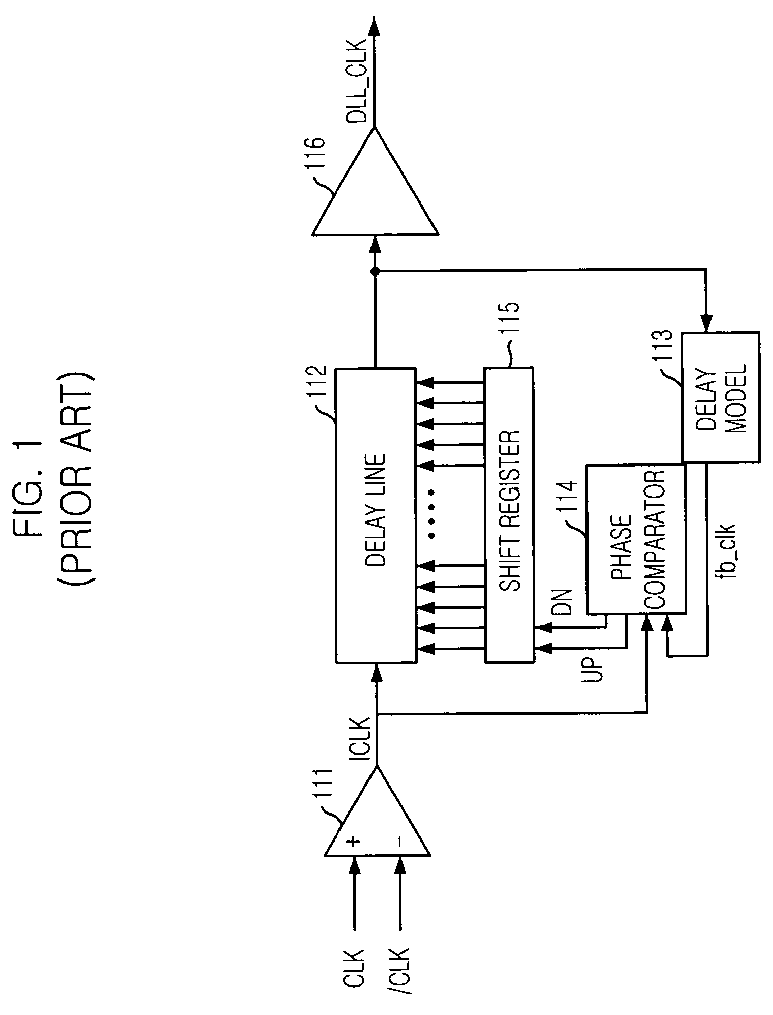
However, when an external clock signal inputted to a semiconductor memory device is converted into an internal clock signal of the semiconductor memory device, a clock skew between the external clock signal and the internal clock signal is generated.
Due to the clock skew, the data cannot be synchronized with the external clock signal when data are outputted from the semiconductor memory device.
Therefore, when the conventional DLL is operated at a high operational frequency, it is difficult to secure characteristics of a signal passed through the delay model 113.
Accordingly, a power consumption of the conventional DLL is also increased.
Therefore, it is not possible to change the constant number according to a variation of the operational frequency.
Therefore, the conventional DLL may not be stably operated when the operational frequency is increased.

Method used


Image

  • Delay locked loop for use in semiconductor memory device and method thereof
  • Delay locked loop for use in semiconductor memory device and method thereof
  • Delay locked loop for use in semiconductor memory device and method thereof

Examples


first embodiment

[0036]FIG. 3 is a block diagram showing a DLL in accordance with the present invention.

[0037] As shown, the DLL includes a first input buffer 311, a second input buffer 312, a multiplexer 316, a multiplexer controller 315, a delay line unit 317, a shift register 314, a phase comparator 313, a divider 318, a delay model 319 and an output buffer 320.

[0038] The first input buffer 311 buffers an external clock signal CLK to generate a rising edge clock signal rclk. A rising edge of the rising edge clock signal rclk corresponds to a rising edge of the external clock signal CLK. Similarly, the second input buffer 312 buffers an inverted version of the external clock signal CLK, i.e., an external clock bar signal / CLK, to generate a falling edge clock signal fclk. A rising edge of the falling edge clock signal fclk corresponds to a falling edge of the external clock signal CLK.

[0039] The multiplexer 316 selects one of the rising edge clock signal rclk and the falling edge clock signal fc...

second embodiment

[0051]FIG. 6 is a block diagram showing a DLL in accordance with the present invention.

[0052] As shown, the DLL includes a first input buffer 611, a second input buffer 612, a multiplexer 616, a multiplexer controller 615, a delay line unit 617, a shift register 614, a phase comparator 613, a divider 618, a delay model 619 and an output buffer 620.

[0053] A structure and an operation of the DLL shown in FIG. 6 are similar to those of the DLL shown in FIG. 3. In comparison with the DLL shown in FIG. 3, the multiplexer controller 615 of the DLL shown in FIG. 6 further receives a most significant bit (MSB) of a delay amount control signal outputted from the shift register 614 and a delay increment control signal UP outputted from the phase comparator 613.

[0054] In case that the delay increment control signal UP is activated when a delay amount added to an input signal of the delay line unit 617 is maximized, it is not possible to increase the delay amount added to the input signal of ...


PUM


Abstract

A delay locked loop (DLL) for generating a delay locked clock signal includes a delay line unit for delaying an external clock signal according to a delay amount control signal to thereby generate the delay locked clock signal; a divider for dividing the delay locked clock signal by a predetermined number determined based on a column address strobe (CAS) latency to thereby generate a divided signal; and a delay line control unit for generating the delay amount control signal based on a result of comparing a phase of the external clock signal and a delayed signal of the divided signal.

Description

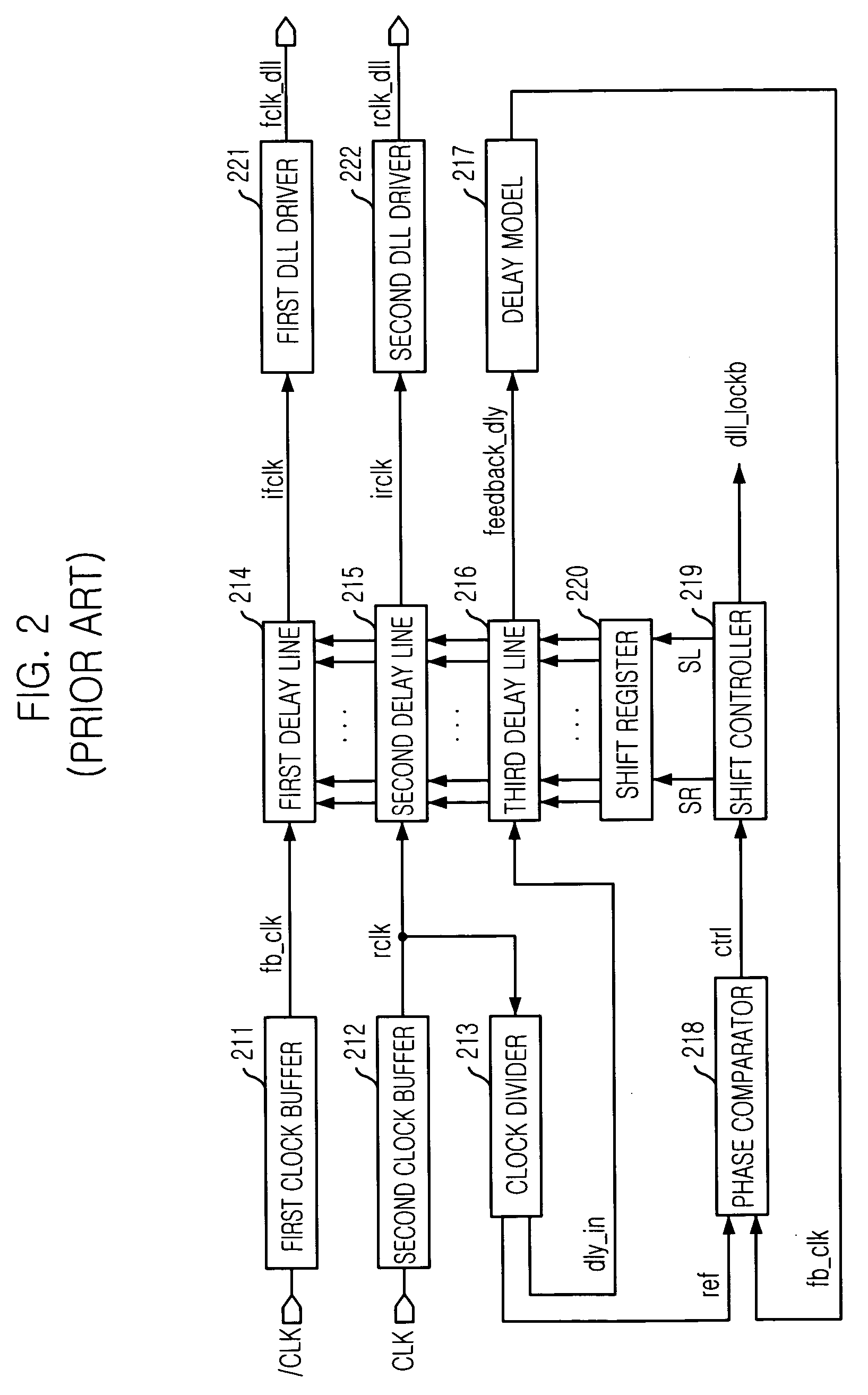
FIELD OF INVENTION [0001] The present invention relates to a delay locked loop (DLL); and, more particularly, to a DLL which is suitable for a high-speed system. DESCRIPTION OF PRIOR ART [0002] Generally, in an electronic circuit system such as a computer system, a clock signal is used as a reference signal for controlling timings of performing various operations. However, when an external clock signal inputted to a semiconductor memory device is converted into an internal clock signal of the semiconductor memory device, a clock skew between the external clock signal and the internal clock signal is generated. Due to the clock skew, the data cannot be synchronized with the external clock signal when data are outputted from the semiconductor memory device. Therefore, a delay locked loop (DLL) is employed in the semiconductor memory device for solving the above-mentioned problem. [0003]FIG. 1 is a block diagram showing a conventional DLL. [0004] As shown, the conventional DLL includes...

Claims


Application Information

Patent Timeline
IPC IPC(8): H03L7/06
CPCH03L7/0814H03L7/089G11C8/00
Inventor LEE, HYUN-WOO
Owner SK HYNIX INC
Learn More