Substrate for a display and method for manufacturing the same

a technology for substrates and displays, applied in the manufacture of electrode systems, applications, electric discharge tubes/lamps, etc., can solve the problems of loss of adhesion of printed and cured metal lines, drawback, etc., to improve the adhesion of printed conductive lines, improve the contact angle of ink jet, and improve the effect of display quality

Inactive Publication Date: 2006-06-22
SAMSUNG SDI CO LTD +1
View PDF11 Cites 11 Cited by
  • Summary
  • Abstract
  • Description
  • Claims
  • Application Information

AI Technical Summary

Benefits of technology

[0010] The present invention relates to improving the adhesion of ink-jet printed conductive lines, for example, ink-jet printed address and bus electrodes, to a ground substrate. The present invention relates to improving the contact angle of ink jet printed conductive lines with respect to a ground substrate so as to implement a high resolution display.

Problems solved by technology

In conventional surface treatment methods, like fluorination with CF4, C2F6, C3F8 or fluoroalkyl-functionalized silanes, the contact angles of 20° to 60° can be achieved, but the drawback is a loss in adhesion of the printed and cured metal lines.

Method used


Image

  • Substrate for a display and method for manufacturing the same
  • Substrate for a display and method for manufacturing the same
  • Substrate for a display and method for manufacturing the same

Examples


Embodiment Construction

[0031] Hereafter, the present invention will now be exemplarily described with reference to the attached drawings.

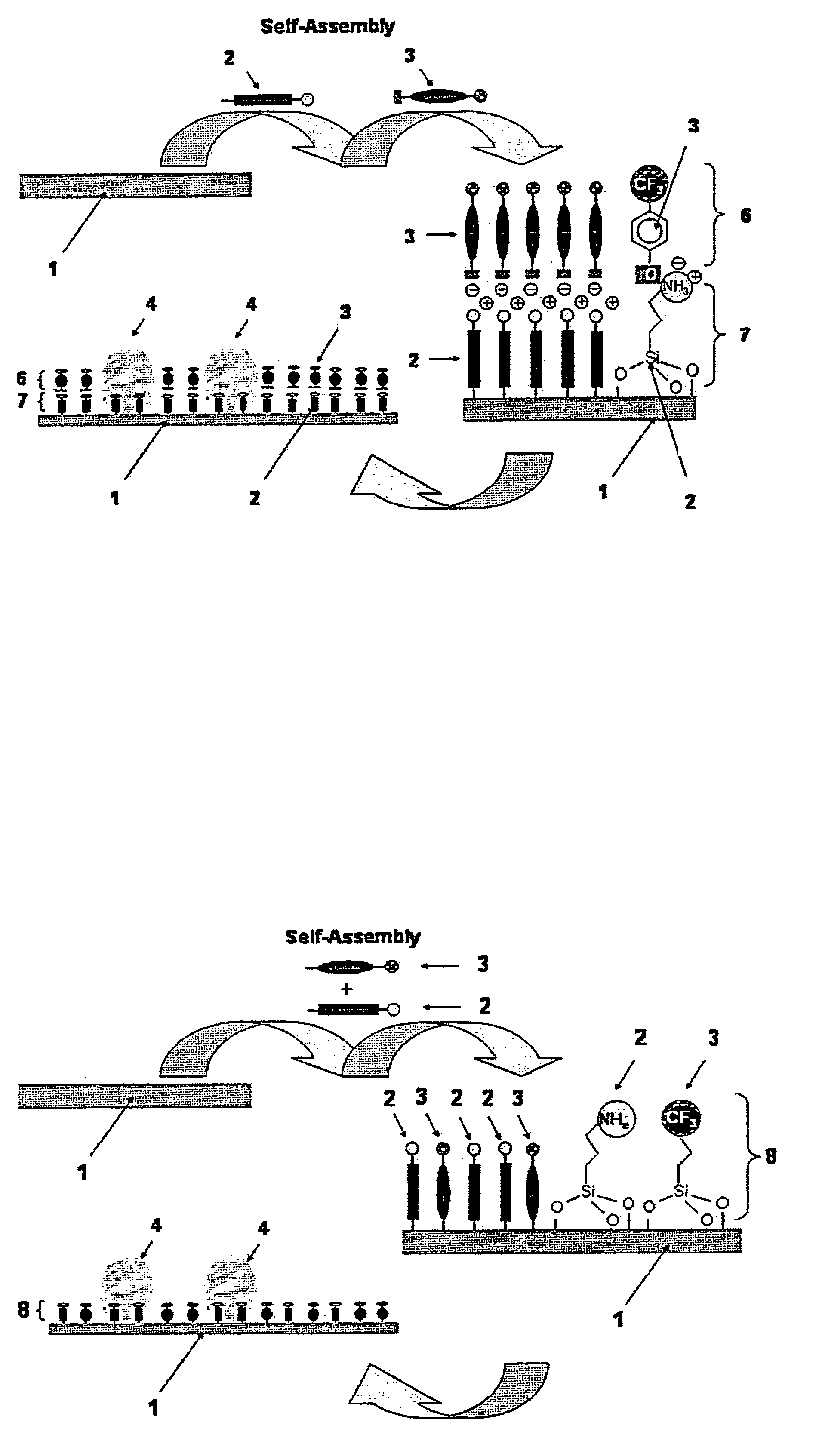
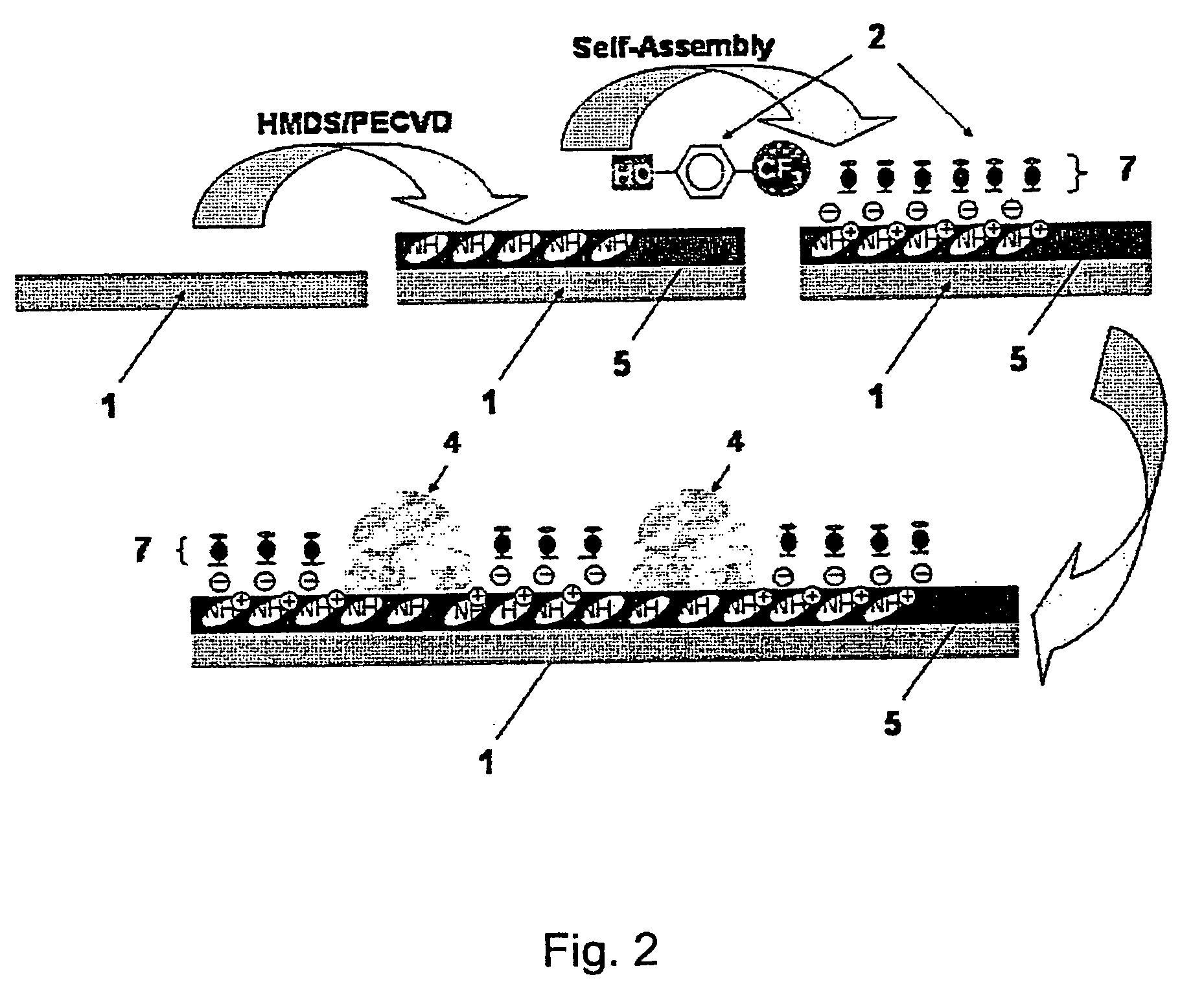
[0032] According to an embodiment of the present invention, a method of manufacturing a substrate for a display having a plurality of conductive lines includes forming at least one intermediate layer between a ground substrate and a plurality of conductive lines by applying metal adhesion promoters and fluorinated precursors.

[0033] At least one intermediate layer can be introduced between the ground substrate and the conductive lines so as to improve the adhesion and the contact angle of ink-jet printed conductive lines to a ground substrate. The metal adhesion promoters and the fluorinated precursors can be sequentially applied, resulting in two intermediate layers of the first layer having the metal adhesion promoters and the second layer having the fluorinated precursors. Alternatively, the metal adhesion promoters and the fluorinated precursors may be simultaneousl...


PUM


Abstract

A substrate for a plasma display panel (PDP) having a plurality of ink-jet printed conductive lines for address and bus electrodes, and a method of manufacturing the substrate are provided. The method includes applying metal adhesion promoter layer to a ground substrate, applying a layer of fluorinated precursors, and applying a plurality of conductive lines. The adhesion of the ink-jet printed conductive lines, i.e. ink-jet printed address and bus electrodes to the ground substrate, and the contact angle of the ink-jet printed conductive lines with respect to the ground substrate are improved, enabling a high resolution display to be manufactured.

Description

CROSS-REFERENCE TO RELATED PATENT APPLICATION AND CLAIM OF PRIORITY [0001] This application claims the benefit of European Patent Application No. 04078333.4, filed on Dec. 7, 2004, in the European Intellectual Property Office, and Korean Patent Application No. 10-2005-0051914, filed on Jun. 16, 2005, in the Korean Intellectual Property Office, the disclosure of which is incorporated herein in its entirety by reference. BACKGROUND OF THE INVENTION [0002] 1. Field of the Invention [0003] The present invention relates to a substrate for a display having a plurality of ink-jet printed conductive lines and a method for manufacturing the same. More particularly, the present invention relates to a substrate for a plasma display panel (PDP) having a plurality of ink-jet printed conductive lines for address and bus electrodes. [0004] 2. Description of the Related Art [0005] Ink-jet printed bus and address electrodes in PDPs are printed with nano particle ink. Silver nano particle ink is comp...

Claims


Application Information

Patent Timeline
Patent Type & Authority Applications(United States)
IPC IPC(8): H01J9/24H01J9/00H01J17/04
CPCB82Y30/00B82Y40/00C09D11/30C09D11/322H01J9/02H01J11/22H01J17/04
Inventor KLYSZCZ, ANDREASSCHAEDIG, MARCUSHUMBS, WERNER
Owner SAMSUNG SDI CO LTD
Why Eureka
Try Eureka