
Polysilicon film, thin film transistor using the same, and method for forming the same

a thin film transistor and polysilicon technology, applied in the direction of coatings, semiconductor devices, chemical vapor deposition coatings, etc., can solve the problems of poor electrical characteristics of poly-si tft, inability to reduce the laser energy requirement in the crystallization process, and difficulty in controlling the number and the location of grain boundaries, etc., to achieve the effect of increasing grain homogeneity and reducing the number of grain boundaries

Active Publication Date: 2006-06-29
AU OPTRONICS CORP
View PDF21 Cites 2 Cited by
  • Summary
  • Abstract
  • Description
  • Claims
  • Application Information

AI Technical Summary

Benefits of technology

[0010] Accordingly, the object of the invention is to provide a method for forming the poly-Si film to reduce the number of the grain boundaries, and to increase the grain homogeneity.
[0011] It is another object of the present invention to provide a process which uses an activated layer to reduce the crystallization energy in manufacturing a transistor.
[0012] It is a further object of the present invention to provide a transistor having a poly-Si channel of good quality to increase the mobility and the transmission.

Problems solved by technology

According to the conventional method, the uncertain crystallizing direction makes it difficult to control the number and the location of the grain boundary.
Besides, more grain boundaries cause worse electrical characteristics of the poly-Si TFT.
To sum up, the conventional method is not capable of controlling the number and the location of the grain boundary, so that the crystallizing direction is uncertain, and it is not capable of reducing the laser energy requirement in the crystallization process, either.

Method used


Image

  • Polysilicon film, thin film transistor using the same, and method for forming the same
  • Polysilicon film, thin film transistor using the same, and method for forming the same
  • Polysilicon film, thin film transistor using the same, and method for forming the same

Examples


Embodiment Construction

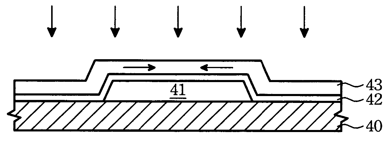
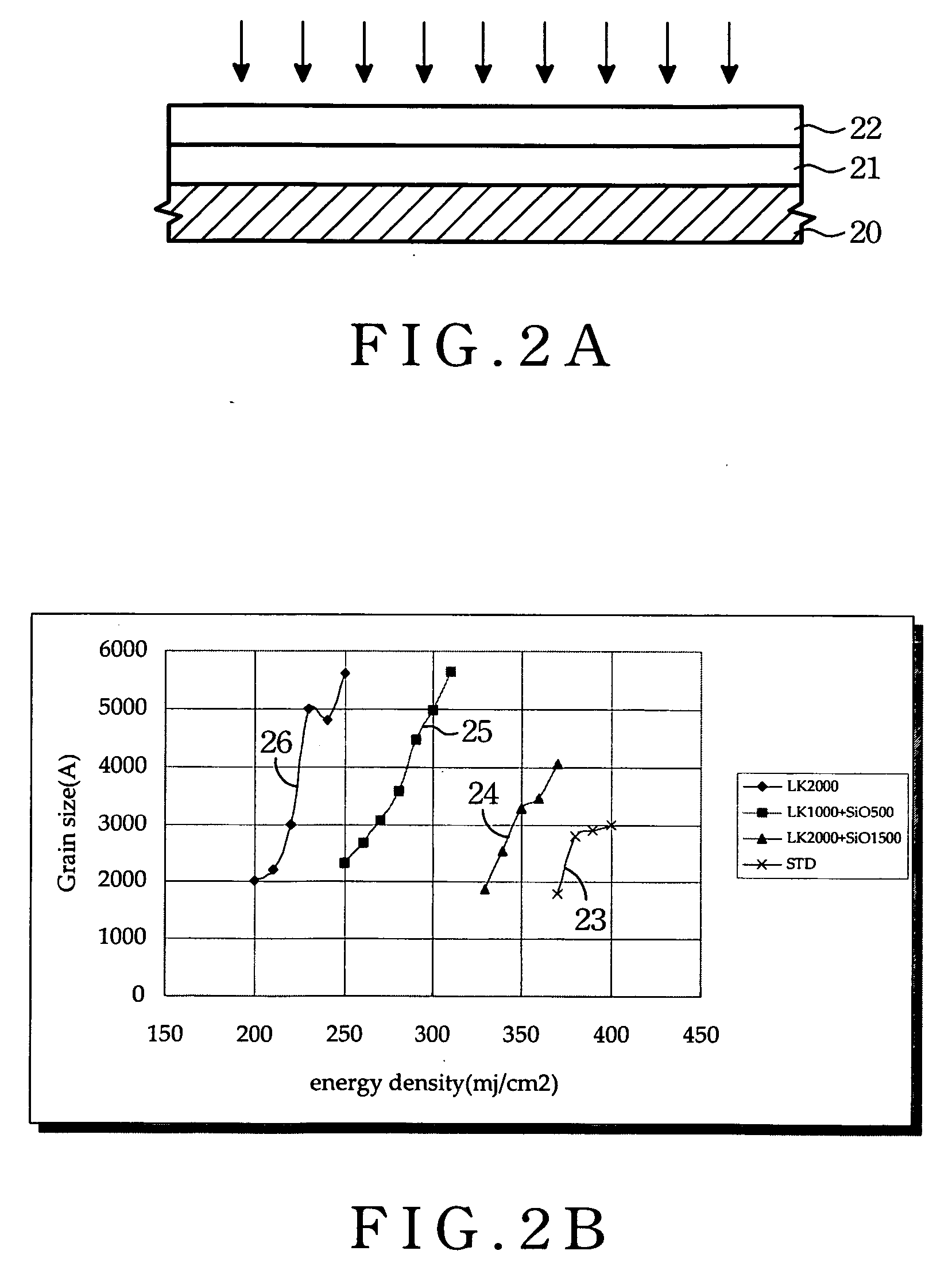
[0028]FIG. 2A shows the basic structure adapting to the method of manufacturing poly-Si film. For reducing crystallization energy, at least one activated layer 21 is positioned on a substrate 20, and an amorphous film 22 is positioned on the activated layer 21. After providing an annealing process for the amorphous silicon film 22, it crystallizes to form a poly-Si film. As shown in FIG. 2B, the grain size of the poly-Si is plotted versus the crystallization energy.

[0029] Refer to FIG. 2B, a curve 23 represents the relation of the grain size of the poly-Si versus the crystallization energy, and the poly-Si is formed by the laser irradiating a structure, which includes: substrate / SiN 500 Å / SiO 1500 Å / amorphous silicon film 500 Å arranged layer by layer. A curve 24 is a result of the laser irradiating the structure, which includes: substrate / activated layer 2000 Å / SiO 1500 Å / amorphous silicon film 500 Å arranged layer by layer. A curve 25 is a result of the laser irradiating the stru...


PUM

PropertyMeasurementUnit
Grain sizeaaaaaaaaaa
Structureaaaaaaaaaa
Energy densityaaaaaaaaaa

Abstract

A crystallizing method for forming a poly-Si film is described as follows. First, forming an activated layer on a substrate, and the molecule structure of the activated layer includes carbon, hydrogen, oxygen and silicon. And then, forming an amorphous silicon film on the activated layer. Finally, performing an annealing process to crystallize the amorphous silicon film and transform it into a poly-Si film.

Description

[0001] This application claims the benefit of Taiwan Application Serial No. 093140572, filed Dec. 24, 2004, the subject matter of which is incorporated herein by reference. BACKGROUND OF THE INVENTION [0002] (1) Field of the Invention [0003] The invention relates to a method for forming a poly-Si film though crystallizing an amorphous silicon film. [0004] (2) Description of the Related Art [0005] A poly-Si material has better attributes than an amorphous silicon material. Because of larger grain size, an electron is easier to move in the poly-Si material. That is, the mobility of the poly-Si material is higher than that of the amorphous silicon material. A transistor made of the poly-Si material has shorter reaction time than a transistor made of the amorphous silicon material. Comparing two liquid crystal displays at the same resolution, the one using a poly-Si TFT occupy less substrate area than the one using an amorphous silicon TFT, so that using the poly-Si TFT can increase the...

Claims


Application Information

Patent Timeline
IPC IPC(8): H01L21/84H01L21/20H01L21/00
CPCH01L21/2026H01L29/66757H01L29/78603H01L29/78675H01L21/02686H01L21/02488H01L21/02502H01L21/02532H01L21/02496H01L21/02595
Inventor PENG, CHIA-TIENCHANG, CHIH-HSIUNG
Owner AU OPTRONICS CORP
Learn More