Multiple resolution optical imager using single size image elements

a multi-resolution, image element technology, applied in the field of image sensors, can solve the problems of affecting image quality and low light sensitivity

Inactive Publication Date: 2006-07-06
LEXMARK INT INC
View PDF27 Cites 14 Cited by
  • Summary
  • Abstract
  • Description
  • Claims
  • Application Information

AI Technical Summary

Benefits of technology

[0023] In still another aspect, the present invention is directed to a single-chip linear image sensor comprising first, second and third rows of same-sized imaging elements having a first resolution, the first and second rows having their imaging elements staggered relative to one another, and the first and third rows having their imaging elements aligned with one another. The image sensor also has first, second and third shift registers, each comprising a plurality of shift register elements. The first and

Problems solved by technology

This smaller element has a lower sensitivity to light and requires a larger exposure

Method used


Image

  • Multiple resolution optical imager using single size image elements
  • Multiple resolution optical imager using single size image elements
  • Multiple resolution optical imager using single size image elements

Examples


Embodiment Construction

[0030] The contents of aforementioned U.S. Pat. No. 6,687,026, U.S. Patent Publication No. 2002 / 0093694, and U.S. Patent Publication No. 2004 / 0109075 are incorporated by reference to the extent necessary to understand the present invention.

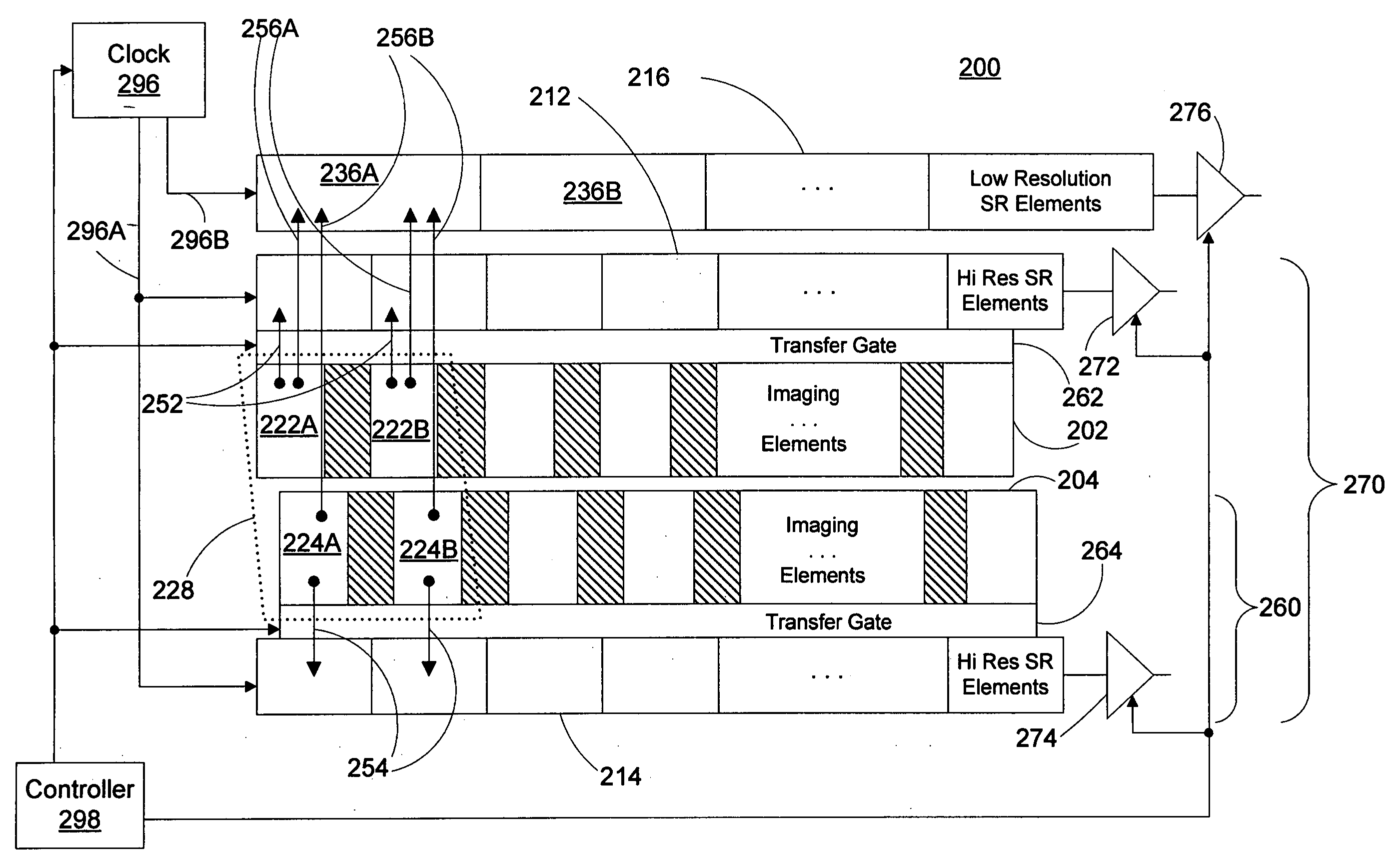
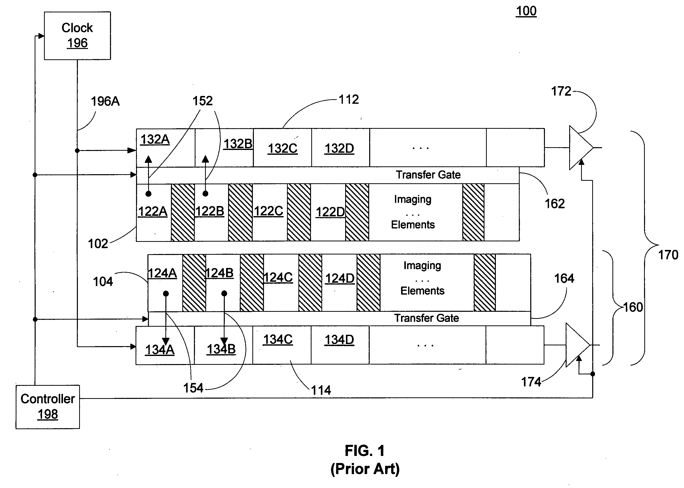
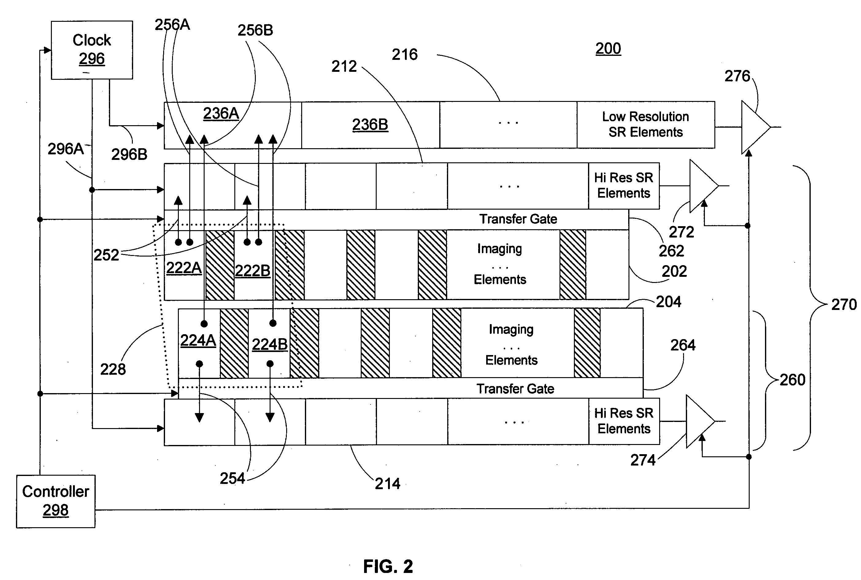
[0031]FIG. 2 shows a portion of an image sensor 200 in accordance with one embodiment of the present invention. FIG. 2 includes all the components of the prior art image sensor of FIG. 1, the common parts being indicated in FIG. 2 by reference numerals having a value 100 greater than their corresponding values in FIG. 1. Thus, image sensor 200 comprises first and second rows 202, 204 of imaging elements, all the imaging element having the same size. The first and second rows 202, 204 connect to respective first and second shift registers 212, 214 via respective first and second transfer gate circuitry 262, 264. The outputs of first and second shift registers 212, 214 feed into respective first and second output amplifiers 272, 274. As depicted by...


PUM


Abstract

An image sensor has two or three rows of imaging elements, all the imaging elements being of the same size. This provides the rows with a native resolution. The image sensor is also provided with three shift registers. First and second shift register elements receive information from respective corresponding imaging element in a first and second row of imagining elements while shift register elements of the third shift register receive information from four imaging elements. The four imaging elements form a super-pixel, allowing the sensor to output information in a low resolution mode, as well a native and a high resolution mode.

Description

CROSS REFERENCES TO RELATED APPLICATIONS [0001] None. STATEMENT REGARDING FEDERALLY SPONSORED RESEARCH OR DEVELOPMENT [0002] None. REFERENCE TO SEQUENTIAL LISTING, ETC. [0003] None. BACKGROUND [0004] 1. Field of the Invention [0005] The present invention is directed to image sensors, such as CIDs, CCDs, and the like. More particularly, it is directed to an image sensor capable of functioning in a plurality of resolution modes. [0006] 2. Description of the Related Art [0007] Image scanners convert a visible image on a document or photograph, or an image in a transparent medium, into an electronic form suitable for copying, storing or processing by a computer. An image scanner can be a separate device or an image scanner may be a part of a copier, part of a facsimile machine, or part of a multipurpose or all-in-one device having printing, scanning, copying and or faxing functionality. Reflective image scanners typically have a controlled source of light, and light is reflected off the...

Claims


Application Information

Patent Timeline
IPC IPC(8): H04N5/335H04N5/341H04N5/372H04N5/376
CPCH04N3/1575H04N3/1581H04N5/23232H04N5/372H04N5/37213H04N23/951H04N25/701H04N25/713H04N25/71H04N25/745
Inventor ANGAL, ADITYA J.CHELVAYOHAN, MAHESANKROGER, PATRICK L.
Owner LEXMARK INT INC
Why Eureka
Try Eureka