Chain resistance pattern and method of forming the same

a resistance pattern and chain resistance technology, applied in the field of chain resistance patterns, can solve problems such as difficulty in locating these various components, and achieve the effect of accurate detection of process errors and maximum measurement results

Inactive Publication Date: 2006-07-06
DONGBU ELECTRONICS CO LTD
View PDF1 Cites 10 Cited by
  • Summary
  • Abstract
  • Description
  • Claims
  • Application Information

AI Technical Summary

Benefits of technology

[0008] An advantage of the present invention is to provide a chain resistance pattern and a method of forming the same, which enables a test pattern to obtain maximum measurement results using minimum area.
[0009] Another advantage of the present invention is to provide a chain resistance pattern and a method of forming the same, which enables accurate detection of process errors.
[0010] An advantage of the present invention is to provide a chain resistance pattern and a method of forming the same, which locates a test pattern in a scribe lane, from which all chain resistances can be measured, by forming a unified chain resistance pattern for measuring a contact resistance.

Problems solved by technology

It is difficult to locate these various components, including both the contact chain resistance and the stack chain resistance, in the scribe lanes of a wafer.

Method used


Image

  • Chain resistance pattern and method of forming the same
  • Chain resistance pattern and method of forming the same
  • Chain resistance pattern and method of forming the same

Examples


Embodiment Construction

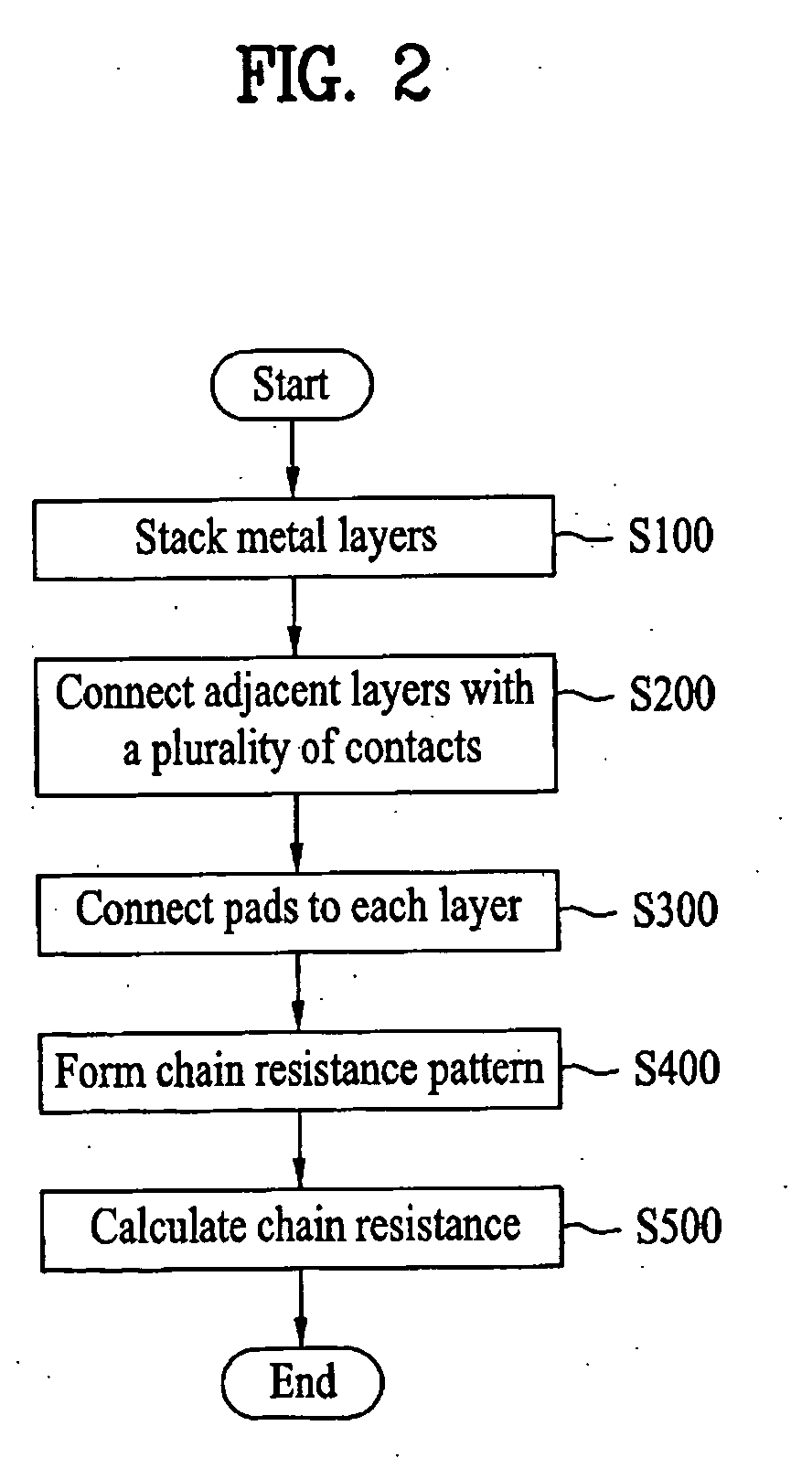
[0018] Reference will now be made in detail to exemplary embodiments of the present invention, examples of which are illustrated in the accompanying drawings. Wherever possible, like reference designations will be used throughout the drawings to refer to the same or similar parts.

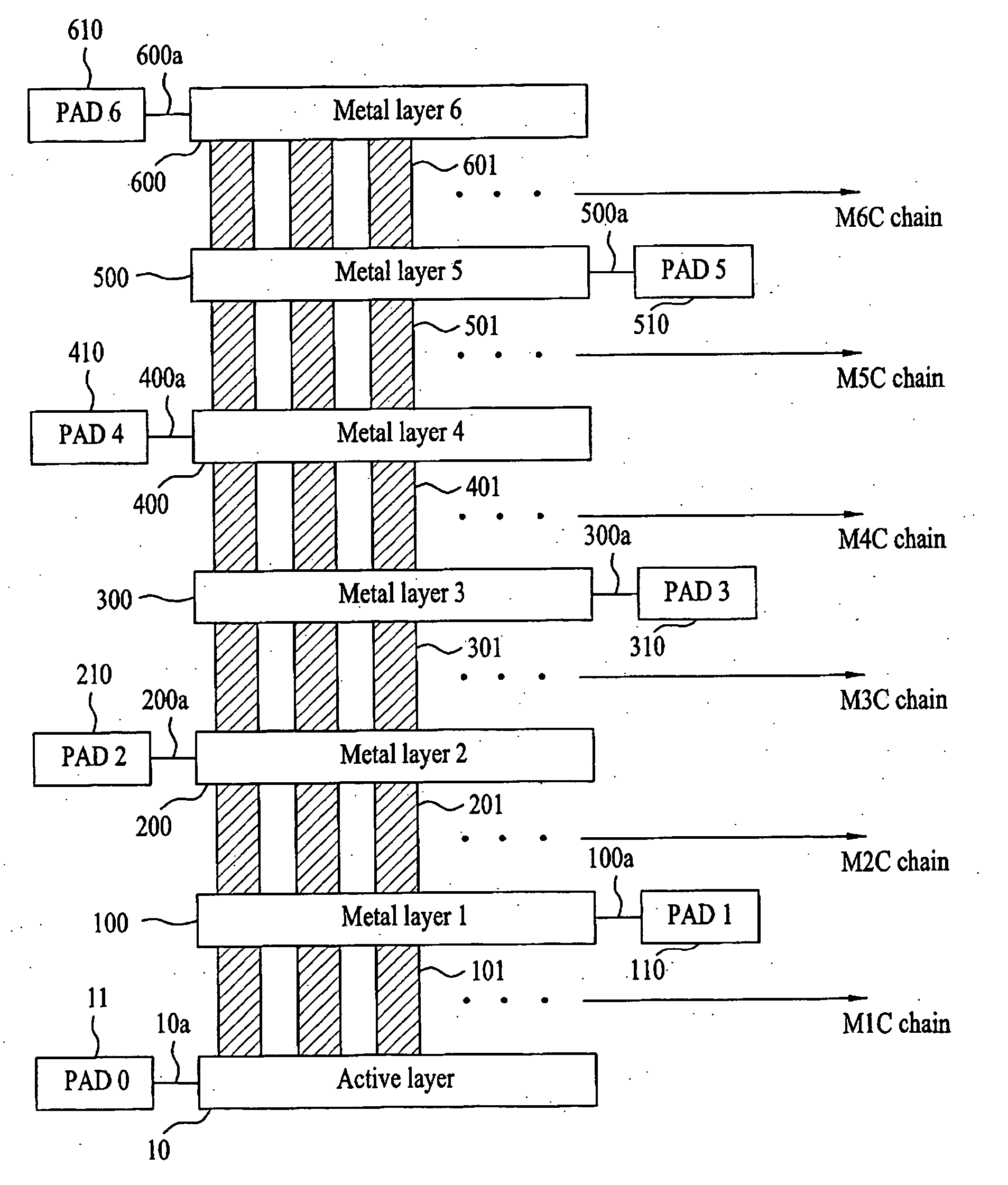
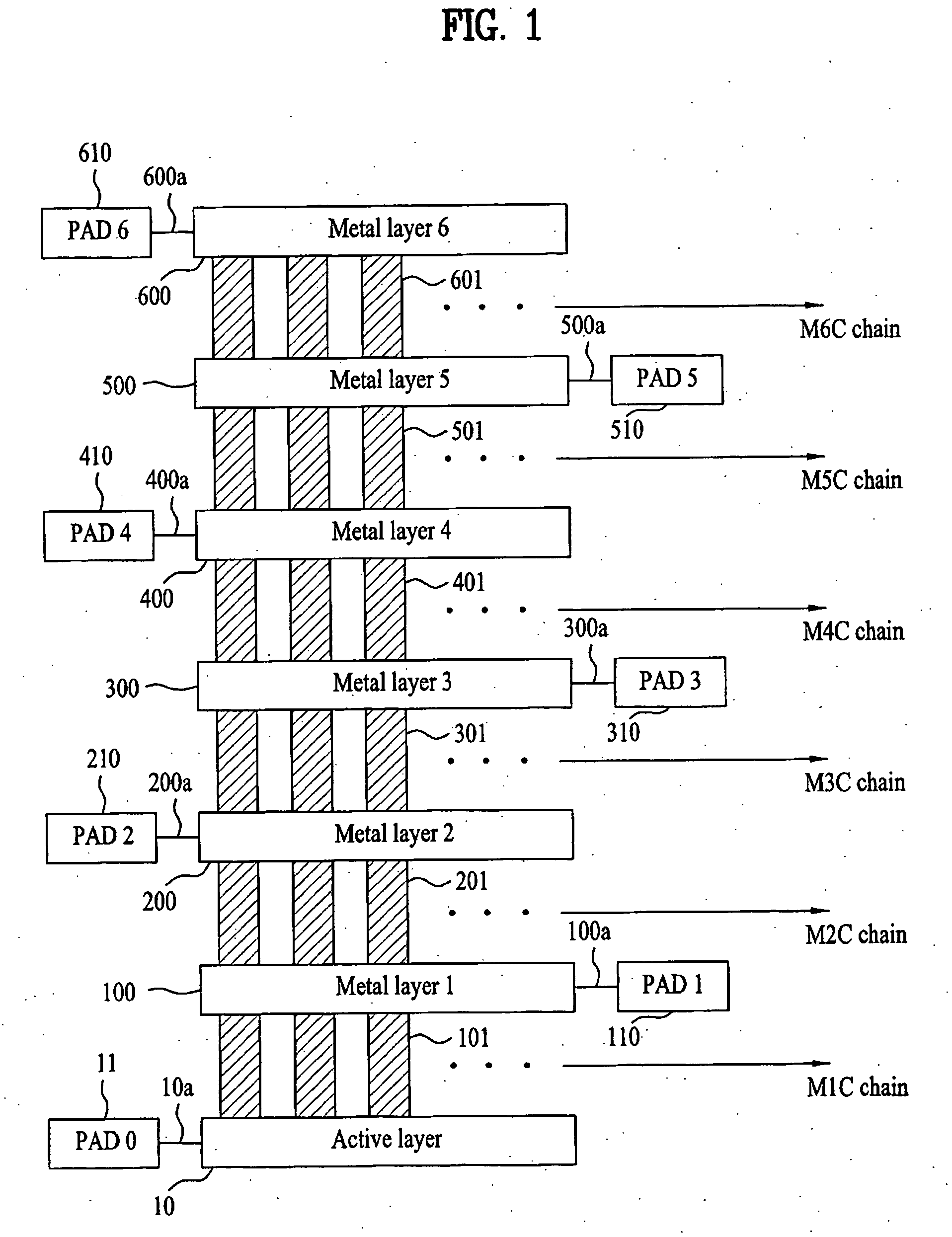
[0019] Referring to FIG. 1, a test pattern including a chain resistance pattern according to an embodiment of the present invention includes a layer stack formed by six conductive layers 100, 200, 300, 400, 500, and 600. The conductive layers are sequentially stacked on an active layer 10, which may be a gate layer, for receiving an externally applied optical signal, and a set of pads 11, 110, 210, 310, 410, 510, and 610 connected to terminals 10a, 100a, 200a, 300a, 400a, 500a, and 600a of the active layer and the six conductive layers, respectively. The conductive layers may be formed of a low-resistance metal. Also, the terminals may be provided at alternating sides of the chain resistance pattern, so th...


PUM


Abstract

A chain resistance pattern and a method of forming the same enable a test pattern to obtain maximum measurement results using minimum area and enable accurate detection of process errors. The chain resistance pattern includes an active layer for receiving an externally applied optical signal, a plurality of conductive layers sequentially stacked on the active layer to form a layer stack, a plurality of contacts, formed between each layer of the layer stack, to electrically connect each pair of adjacently disposed layers of the layer stack, and a pad connected to each layer of the layer stack.

Description

[0001] This application claims the benefit of Korean Patent Application No. 10-2004-0116636, filed on Dec. 30, 2004, which is hereby incorporated by reference for all purposes as if fully set forth herein. BACKGROUND OF THE INVENTION [0002] 1. Field of the Invention [0003] The present invention relates to semiconductor devices, and more particularly, to a chain resistance pattern and a method of forming the same, which enables an improved test pattern to obtain maximum measurement results using minimum layout area and which enables accurate detection of process errors. [0004] 2. Discussion of the Related Art [0005] In the field of semiconductor device manufacture, in-process tests are performed to measure various resistances using test patterns. The test patterns of the related art for contact resistance measurement are based on a chain resistance or a Kelvin resistance. A contact chain resistance pattern obtains an actual resistance value by measuring a sample device, e.g., a unit ...

Claims


Application Information

Patent Timeline
Patent Type & Authority Applications(United States)
IPC IPC(8): H01L21/66G01R31/26
CPCG01R31/2831G01R31/2884H01L22/34H01L27/04
Inventor JUNG, MYUNG JIN
Owner DONGBU ELECTRONICS CO LTD
Why Eureka
Try Eureka