
Method for manufacturing semiconductor device

Inactive Publication Date: 2006-07-06
DONGBU ELECTRONICS CO LTD
View PDF8 Cites 3 Cited by
  • Summary
  • Abstract
  • Description
  • Claims
  • Application Information

AI Technical Summary

Benefits of technology

[0008] An object of the present invention is to provide a method for manufacturing a semiconductor device, which prevents copper contamination.

Problems solved by technology

Typically in performing a copper-related process such as a copper line formation as part of a back end-of-line process, a rear surface of a substrate can be contaminated with copper.
Thus, since a tetraethylorthosilicate-based oxide layer may be exposed during spacer and / or copper line formation, it can be difficult to prevent the contamination of copper.

Method used


Image

  • Method for manufacturing semiconductor device
  • Method for manufacturing semiconductor device
  • Method for manufacturing semiconductor device

Examples


Embodiment Construction

[0014] Reference will now be made in detail to exemplary embodiments of the present invention, examples of which are illustrated in the accompanying drawings. Wherever possible, like reference designations will be used throughout the drawings to refer to the same or similar parts.

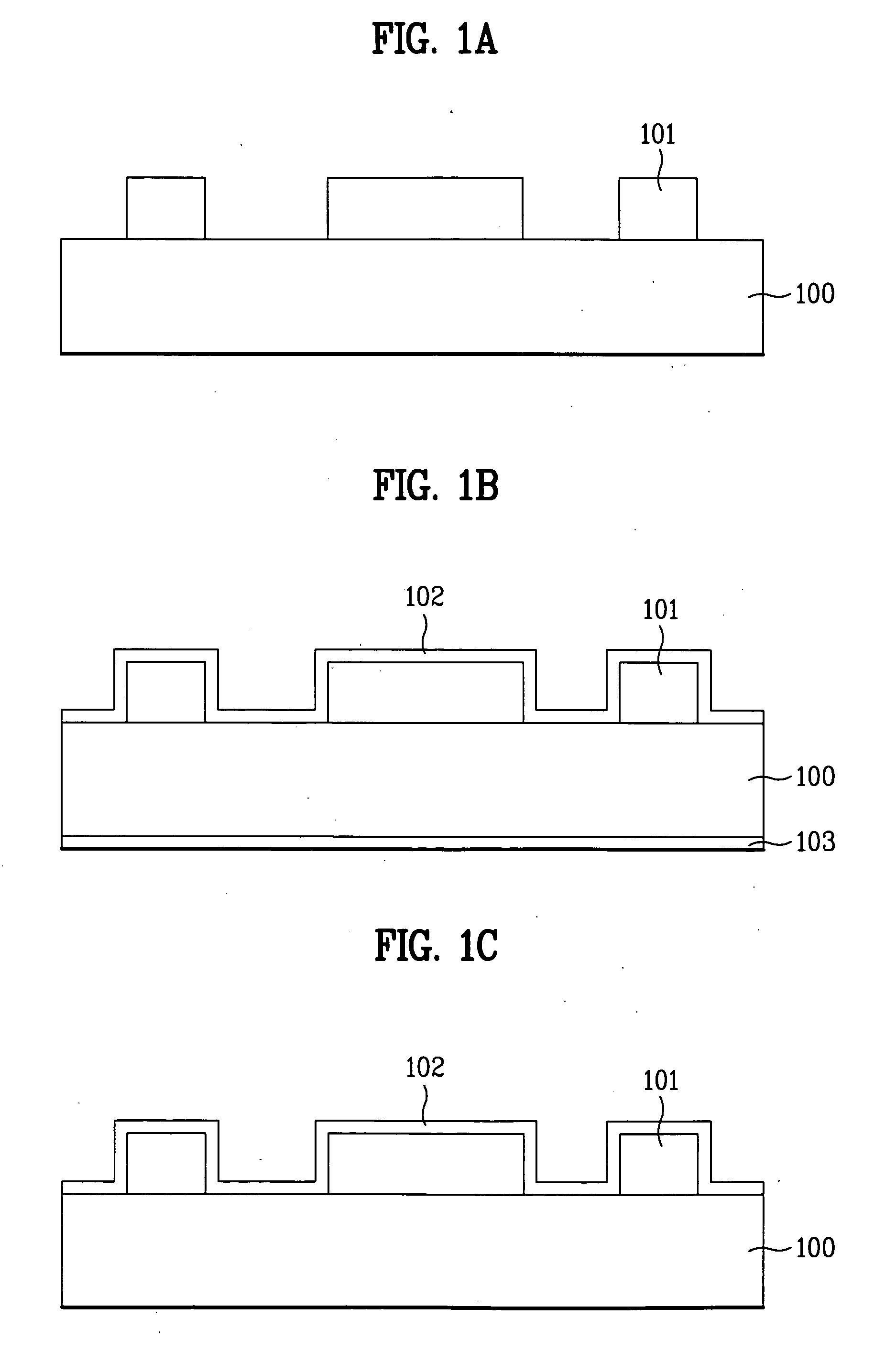
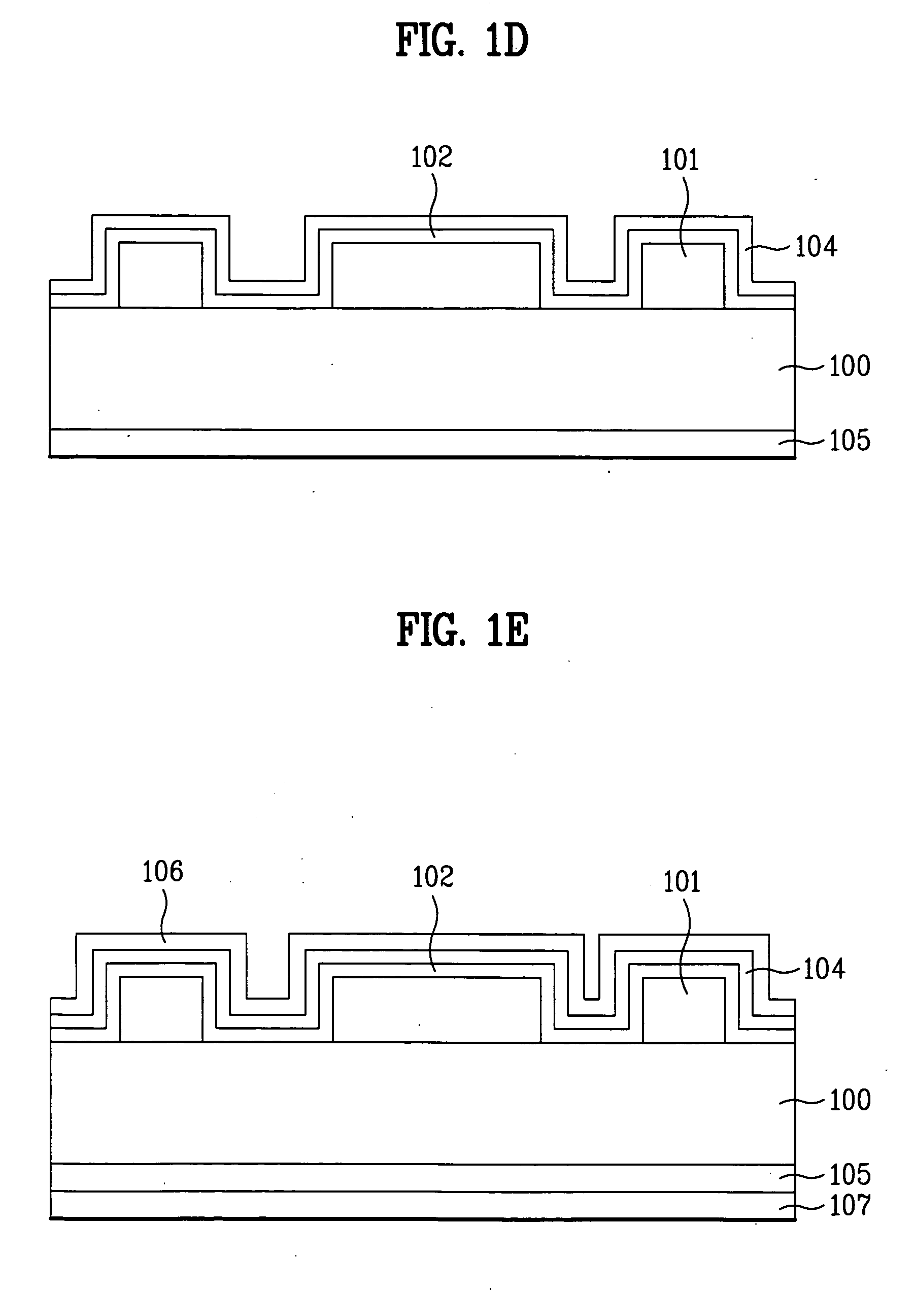
[0015]FIGS. 1A-1G respectively illustrate sequential process steps of a method for manufacturing a semiconductor device according to the present invention.

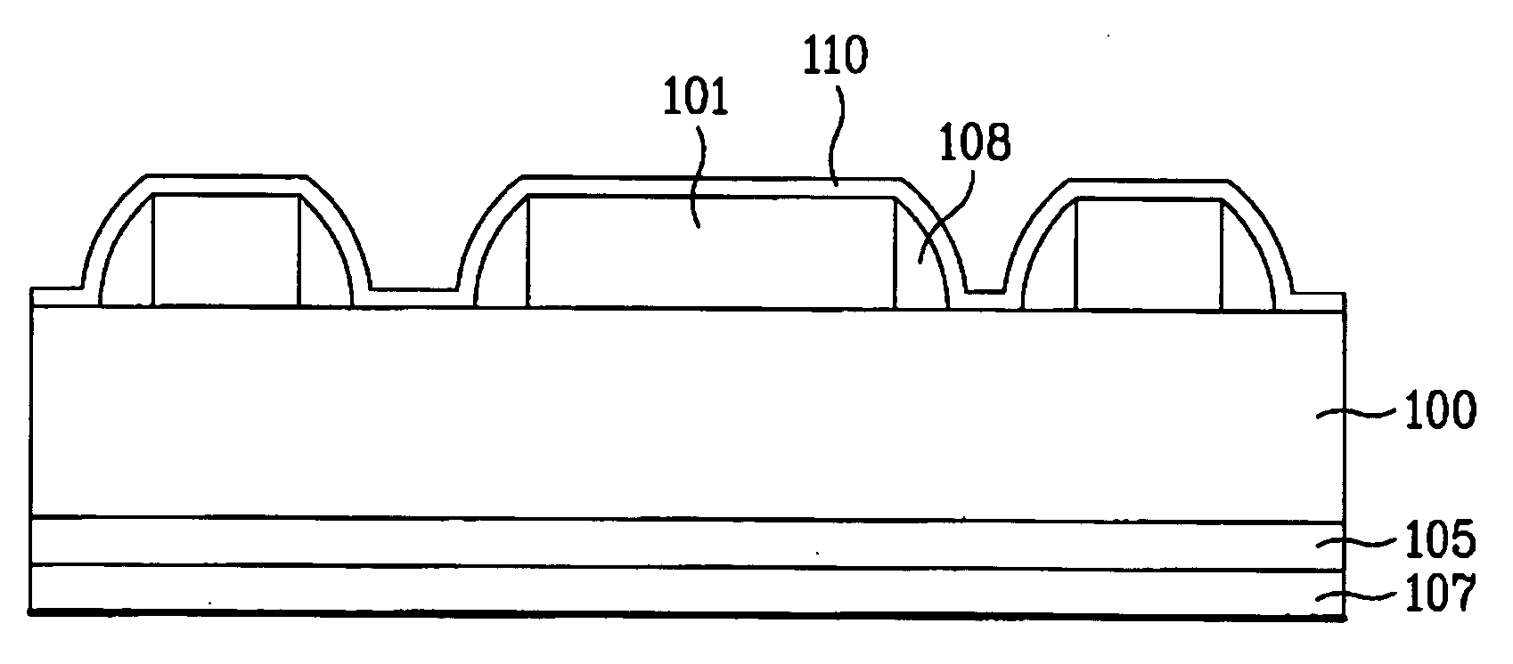
[0016] Referring to FIG. 1A, a polysilicon layer is deposited on an entire front surface of a substrate 100 and is then selectively etched (e.g., by photolithographic patterning of a photoresist, and etching the polysilicon layer using the patterned photoresist as an etching mask), thereby forming a gate electrode 101. Generally, although not shown in FIG. 1A, the polysilicon layer is blanket deposited onto substrate 100 having a thin gate oxide layer in the active areas, and both the polysilicon layer and the gate oxide layer are etched to form gate el...


PUM


Abstract

A method for manufacturing a semiconductor device reduces or prevents copper contamination. The method includes forming a gate electrode on a substrate; forming a first oxide layer on a front surface of the substrate including the gate electrode; depositing a nitride layer (simultaneously) on the first oxide layer and a rear surface of the substrate; depositing a second oxide layer on the nitride layer; removing the second oxide layer from the rear surface of the substrate; and forming spacers at sides of the gate electrode by etching the second oxide layer, the nitride layer, and the first oxide layer.

Description

[0001] This application claims the benefit of Korean Patent Application No. 10-2004-0117605, filed on Dec. 31, 2004, which is hereby incorporated by reference as if fully set forth herein. BACKGROUND OF THE INVENTION [0002] 1. Field of the Invention [0003] The present invention relates to a semiconductor device, and more particularly, to a method for manufacturing a semiconductor device that reduces or prevents copper contamination. [0004] 2. Discussion of the Related Art [0005] Typically in performing a copper-related process such as a copper line formation as part of a back end-of-line process, a rear surface of a substrate can be contaminated with copper. That is, since copper exhibits great diffusivity in certain materials such as single-crystal silicon, copper particles penetrating through the rear surface of the substrate may be diffused to a front surface of the substrate. Various methods for removing the copper from the rear surface of the substrate are proposed. [0006] In m...

Claims


Application Information

Patent Timeline
IPC IPC(8): H01L21/3205H01L21/44
CPCH01L21/31633H01L21/3185H01L21/76829Y10S438/928H01L21/022H01L21/02271H01L21/0217H01L21/18H01L21/31H01L21/28
Inventor KIM, JEA HEE
Owner DONGBU ELECTRONICS CO LTD
Learn More