Surface mount LED

a light-emitting diode and surface-mount technology, applied in the direction of discharge tube/lamp details, discharge tube luminescnet screens, electric discharge lamps, etc., can solve the problems of repeated thermal expansion and contraction of light-emitting resin, peeling at the contact interface, electrical property failure, etc., to suppress interface peeling, strong intimate contact force, effect of suppressing peel

Inactive Publication Date: 2006-07-13
STANLEY ELECTRIC CO LTD
View PDF10 Cites 9 Cited by
  • Summary
  • Abstract
  • Description
  • Claims
  • Application Information

AI Technical Summary

Benefits of technology

[0020] As a result, compared to the contact interface between the sealant resin and the circuit pattern, the intimate contact interface between the sealant resin and the exposed insulator has a stronger intimate contact force. Therefore, it is possible to suppress peel in high-temperature mounting environments and in practical use even when a thermal stress acts on the interface between the sealant resin and the insulator.
[0021] Accordingly, it is possible to suppress interface peel between the circuit pattern partly formed on the bottom in the recess and the conductive adhesive applied for electrically connecting the circuit pattern with the LED chip. Thus, a reliable surface-mounted LED that causes little or no electrical property failure can be provided.

Problems solved by technology

This difference and other factors may cause a stress that results in peel at a contact interface between the circuit pattern and the resin.
In this case, the light transmissive resin may peel off the circuit pattern, possibly resulting in an electrical property failure.
Even after the surface-mounted LED is mounted on the component-mounting board, the repetition of switching the LED on / off can cause repeated thermal expansion and contraction of the light transmissive resin.
In addition, the stress at that time may exert the same action as described above and possibly result in an electrical property failure.

Method used


Image

  • Surface mount LED
  • Surface mount LED
  • Surface mount LED

Examples


Embodiment Construction

[0031] Exemplary embodiments of the invention will now be described with reference to FIGS. 1-7 in detail (using the same reference numerals to denote the same or similar parts). The embodiments described below are examples of the invention and include various technical features. The scope of the invention is not limited to these embodiments.

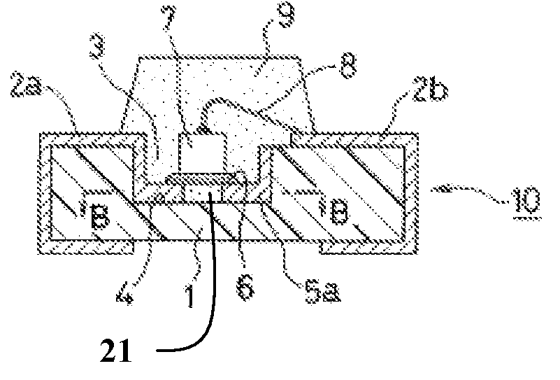
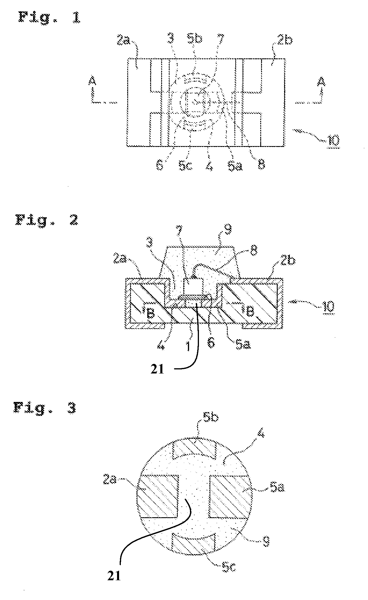
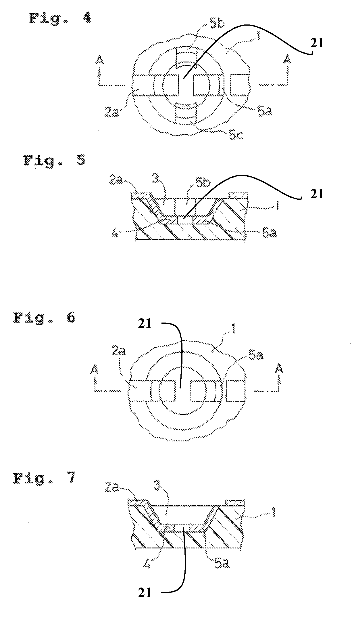
[0032]FIG. 1 is a top view illustrative of an embodiment of a surface-mount LED made in accordance with principles of the invention, and FIG. 2 is a cross-sectional view taken along line A-A in FIG. 1. An insulator 1 has an upper surface with opposite ends, on which a pair of circuit patterns 2a, 2b are formed. The circuit patterns 2a, 2b can extend from edges, around sides, to the lower surface of the insulator 1.

[0033] A recess 3 can be provided at the upper surface of the insulator 1. The recess can be provided at the approximate center of and in the upper surface of the insulator 1. The circuit pattern 2a can extend around part of the inne...


PUM


Abstract

In a surface mount LED, circuit patterns can be formed on selective portions of the bottom and inner circumferential surfaces of a recess in a substrate in which an LED chip is mounted. A sealant material composed of a light transmissive resin can be applied to cover the LED chip for sealing. An intimate contact interface is formed between the material of the insulator/substrate which is exposed at a portion with no circuit pattern formed thereon, and the light transmissive resin. The strength of intimate contact can be enhanced to prevent the circuit patterns and conductive adhesive from peeling off at an interface therebetween.

Description

[0001] This application claims the priority benefit under 35 U.S.C. § 119 of Japanese Patent Application No. 2005-002705 filed on Jan. 7, 2005, the disclosure of which is hereby incorporated in its entirety by reference. BACKGROUND OF THE INVENTION [0002] 1. Field of the Invention [0003] The invention relates to a surface-mount light-emitting diode (LED). More particularly, the invention relates to a surface-mounted LED including an LED chip mounted in a recess provided in a substrate, in which a sealant resin is applied to seal the LED chip. [0004] 2. Description of the Related Art [0005] A conventional surface-mounted LED may have the structure shown inFIGS. 8 and 9. FIG. 8 is a top view and FIG. 9 is a cross-sectional view taken along line A-A in FIG. 8. It includes a pair of circuit patterns 51a, 51b formed in the upper surface of an insulator 50 at both opposite ends. The circuit patterns 51a, 51b extend from edges of the insulator 50 to the lower surface around sides of the in...

Claims


Application Information

Patent Timeline
Patent Type & Authority Applications(United States)
IPC IPC(8): H01L33/00H01L29/22H01L33/50H01L33/56H01L33/60H01L33/62
CPCH01L33/486H01L33/62H01L2224/48091H01L2224/48227H01L2224/48465H01L2224/73265H01L2924/01079H01L2924/00014H01L2224/32225H01L2924/00H01L2924/12041H01L2924/15153H01L2924/00012H01L24/73
Inventor WATANABE, SEISHIOGAWA, YOSHIHIRO
Owner STANLEY ELECTRIC CO LTD
Why Eureka
Try Eureka