Quasi-hydrophobic Si-Si wafer bonding using hydrophilic Si surfaces and dissolution of interfacial bonding oxide

a hydrophobic si and surface technology, applied in the field of semi-hydrophobic si-si wafer bonding, can solve the problems of incompatibility with an oxide-free bonded interface, less well developed technique, and more difficult and less well developed techniqu

Inactive Publication Date: 2006-07-13
GLOBALFOUNDRIES INC
View PDF4 Cites 83 Cited by
  • Summary
  • Abstract
  • Description
  • Claims
  • Application Information

AI Technical Summary

Benefits of technology

[0026] It should be noted that the aspect of the present invention relating to Si-to-Si bonding is used to best advantage when the Si surfaces at the bonded

Problems solved by technology

Such direct Si-to-Si bonding is normally achieved with hydrophobic bonding, a more difficult and less well developed technique than the more commonly used hydrophilic bonding.
Hydrophobic bonding is a relatively difficult technique for several reasons.
In addition, the widely used surface plasma treatments developed to allow room temperature bonding typically introduce surface oxygen, making them incompatible with an oxide-free bonded interface.
Bonding at higher temperatures also can present difficulties, since most cleaving processes (used to separate the bonded layer from the wafer to which it was originally attached) are thermally activated and start occurring in the same temperature range as the bonding.
“Stability of interfacial oxide layers during silicon wafer bonding,

Method used


Image

  • Quasi-hydrophobic Si-Si wafer bonding using hydrophilic Si surfaces and dissolution of interfacial bonding oxide
  • Quasi-hydrophobic Si-Si wafer bonding using hydrophilic Si surfaces and dissolution of interfacial bonding oxide
  • Quasi-hydrophobic Si-Si wafer bonding using hydrophilic Si surfaces and dissolution of interfacial bonding oxide

Examples


example

[0058] This example illustrates how the method of the present invention was used to remove an interfacial oxide present at the bonded interface between a (100)-oriented Si layer and a (110)-oriented Si handle wafer. Interfacial oxide removal was established by comparing transmission electron micrograph (TEM) images (FIG. 7) and optical reflectance data (FIG. 8) before and after annealing.

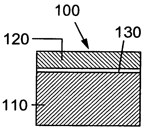
[0059]FIG. 7A shows a TEM image of a substrate structure 300 analogous to 100 of FIG. 2A or 5A, with (110)-oriented Si handle wafer 320, (100)-oriented Si layer 310 having a thickness of 160 nm, and interfacial oxide layer 330 having a thickness of 2-3 nm remaining after a 2 hour bonding anneal at 1000° C. The gray-scale color contrast between Si layer 310 and Si handle wafer 320 results from the difference in their crystal orientations.

[0060] The solid trace in FIG. 8A shows reflectance vs. wavelength data for the substrate structure 300. The oscillations in the wavelength range 400-800 nm (absen...


PUM


Abstract

The present invention provides a method for removing or reducing the thickness of ultrathin interfacial oxides remaining at Si—Si interfaces after silicon wafer bonding. In particular, the invention provides a method for removing ultrathin interfacial oxides remaining after hydrophilic Si—Si wafer bonding to create bonded Si—Si interfaces having properties comparable to those achieved with hydrophobic bonding. Interfacial oxide layers of order of about 2 to about 3 nm are dissolved away by high temperature annealing, for example, an anneal at 1300°-1330° C. for 1-5 hours. The inventive method is used to best advantage when the Si surfaces at the bonded interface have different surface orientations, for example, when a Si surface having a (100) orientation is bonded to a Si surface having a (110) orientation. In a more general aspect of the invention, the similar annealing processes may be used to remove undesired material disposed at a bonded interface of two silicon-containing semiconductor materials. The two silicon-containing semiconductor materials may be the same or different in surface crystal orientation, microstructure (single-crystal, polycrystalline, or amorphous), and composition.

Description

RELATED APPLICATIONS [0001] This application is related to attorney docket YOR920040659US1 entitled “Method For Fabricating Low-Defect Density Changed Orientation Si”, which application is being filed on the same date as the present application. FIELD OF THE INVENTION [0002] The present invention generally relates to semiconductor wafer bonding, and more particularly to methods of silicon-to-silicon, i.e., Si—Si, wafer bonding in which two wafers having different Si surface orientations are joined and processed in such a manner as to produce a bonding interface that is clean and substantially free of any interfacial oxide. BACKGROUND OF THE INVENTION [0003] Semiconductor device technology is increasingly relying on specialty Si-based substrates to improve the performance of complementary metal oxide semiconductor (CMOS) devices, such as nFETs (i.e., n-channel MOSFETs) or pFETs (i.e., p-channel MOSFETs). For example, the strong dependence of carrier mobility on silicon orientation ha...

Claims


Application Information

Patent Timeline
IPC IPC(8): H01L21/46
CPCH01L21/187H01L21/76251
Inventor DE SOUZA, JOEL P.OTT, JOHN A.REZNICEK, ALEXANDERSADANA, DEVENDRA K.SAENGER, KATHERINE L.
Owner GLOBALFOUNDRIES INC
Why Eureka
Try Eureka