BIPOLAR TRANSISTOR WITH COLLECTOR HAVING AN EPITAXIAL Si:C REGION

a bipolar transistor and collector technology, applied in the field of bipolar transistors, can solve the problems of serious device operational limitations, achieve the effects of reducing parasitic ccb, controlling carbon profile and location, and suppressing the out-diffusion of collector implant dopants

Inactive Publication Date: 2006-07-13
IBM CORP
View PDF2 Cites 5 Cited by
  • Summary
  • Abstract
  • Description
  • Claims
  • Application Information

AI Technical Summary

Benefits of technology

[0010] The present invention provides a structure where C is incorporated into the collector of a bipolar device by a method which does not include C ion implantation. In the present invention, C is incorporated into the collector by epitaxy in a perimeter trench (or recess) etched into the collector to better control the carbon profile and location. The carbon suppresses the out-diffusion of the collector implant dopants from the intrinsic device toward its perimeter, which results in a lower parasitic CCB. The trench (or recess) is formed by etching portions of the collector using the trench isolation regions that helped to define the collector and a patterned layer over the center part of the collector as masks. Si:C is then grown using selective epitaxy inside the trench (or recess) to form a Si:C region with sharp and well-defined edges. The Si:C region is positioned next to each trench isolation region that was used to define the collector. The depth, width and C content can be optimized to control and tailor the collector implant diffusion and to reduce the perimeter component of parasitic CCB.

Problems solved by technology

As the vertical dimensions of the bipolar transistor are scaled more and more, serious device operational limitations have been encountered.

Method used


Image

  • BIPOLAR TRANSISTOR WITH COLLECTOR HAVING AN EPITAXIAL Si:C REGION
  • BIPOLAR TRANSISTOR WITH COLLECTOR HAVING AN EPITAXIAL Si:C REGION
  • BIPOLAR TRANSISTOR WITH COLLECTOR HAVING AN EPITAXIAL Si:C REGION

Examples


Embodiment Construction

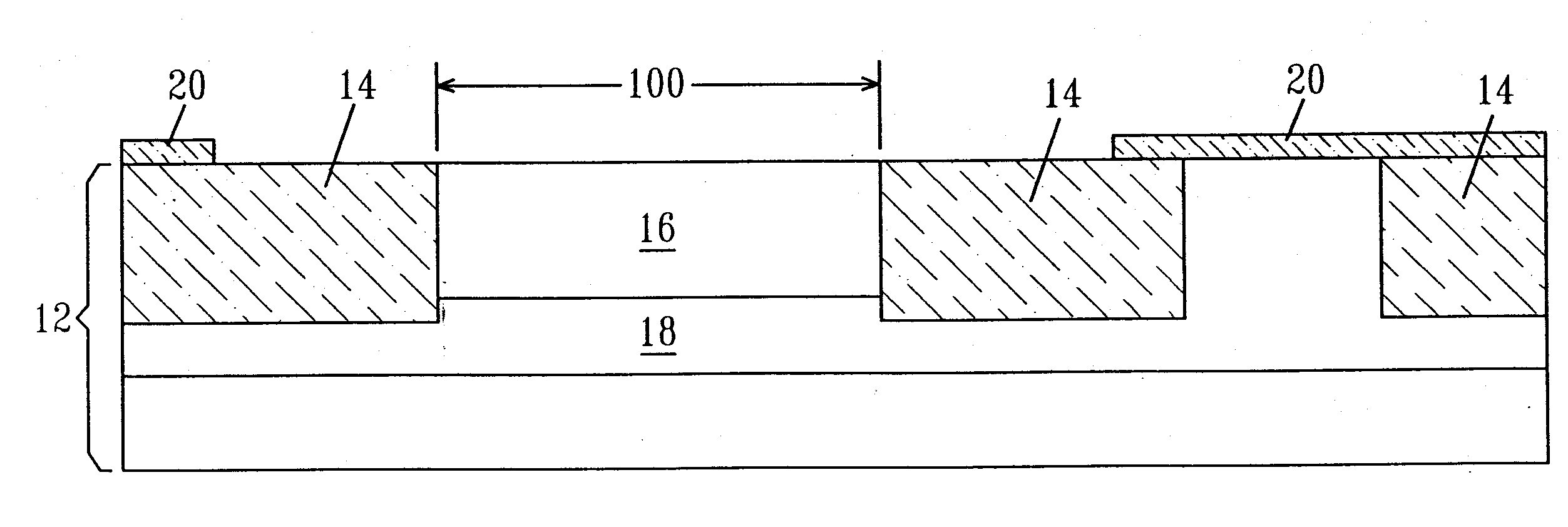
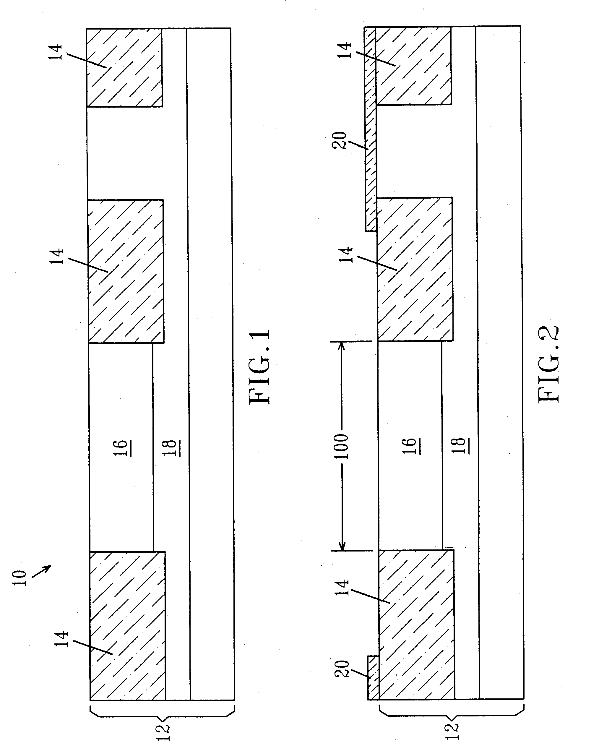
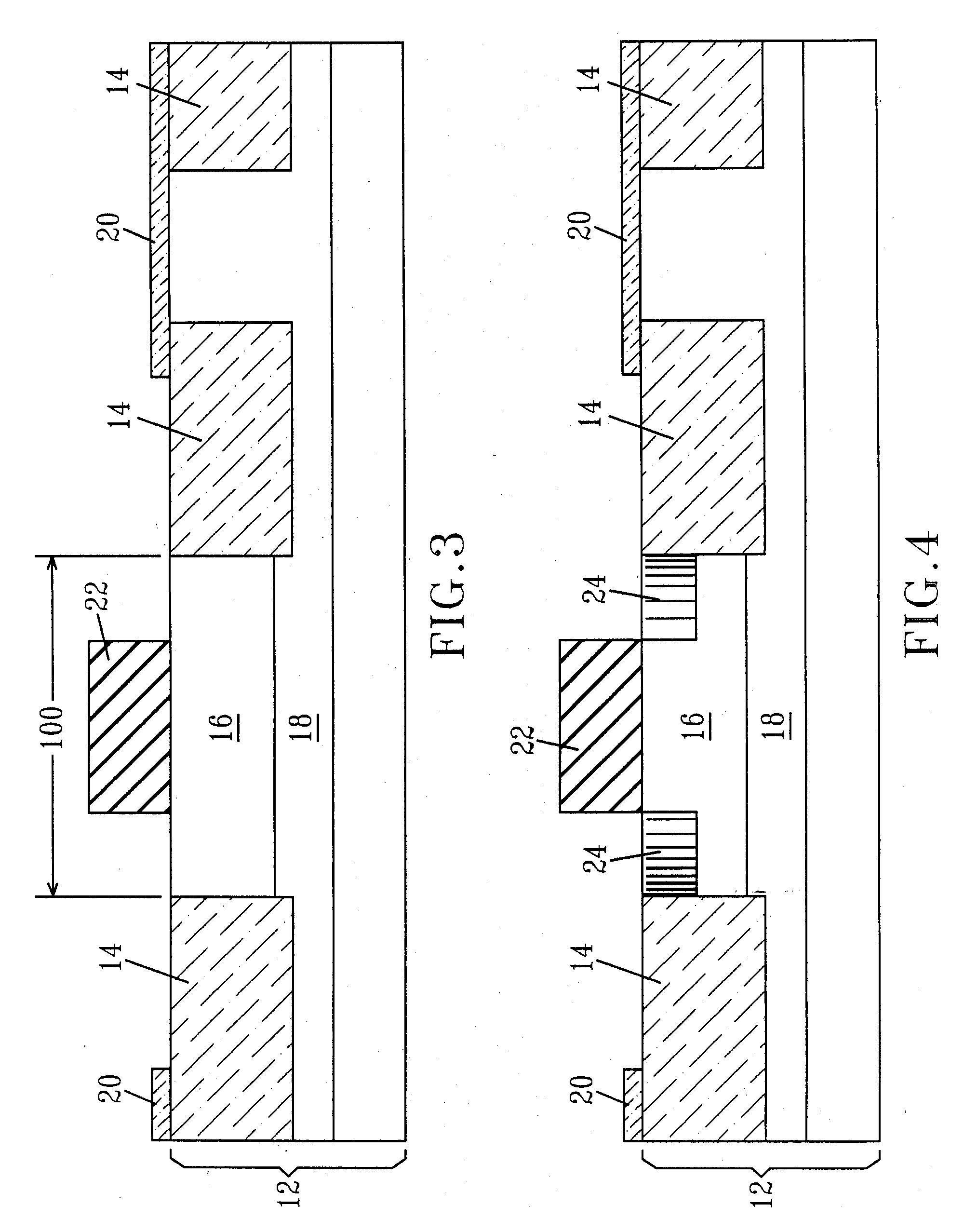
[0029] The present invention, which provides a bipolar transistor with a collector having an epitaxial Si:C region and a method of fabricating the same, will now be described in greater detail by referring to the drawings that accompany the present application. The drawings are provided for illustrative purposes and thus they are not drawn to scale.

[0030] The inventive method of forming a bipolar device with a collector having an epitaxial Si:C region begins with first providing the initial structure 10 shown in FIG. 1. The initial structure 10 includes a Si-containing substrate 12 having trench isolation regions 14 formed therein. The Si-containing substrate includes any semiconductor material that includes silicon. Illustrative examples of such Si-containing semiconductor materials include, but are not limited to: Si, SiGe, a silicon-on-insulator (SOI), or a silicon germanium-on-insulator (SGOI). Alternatively, the Si-containing substrate 12 may be a Si layer such as epitaxial Si...


PUM


Abstract

A structure and method where C is incorporated into the collector region of a heterojunction bipolar device by a method which does not include C ion implantation are provided. In the present invention, C is incorporated into the collector by epitaxy in a perimeter trench etched into the collector region to better control the carbon profile and location. The trench is formed by etching the collector region using the trench isolation regions and a patterned layer over the center part of the collector as masks. Then, Si:C is grown using selective epitaxy inside the trench to form a Si:C region with sharp and well-defined edges. The depth, width and C content can be optimized to control and tailor the collector implant diffusion and to reduce the perimeter component of parasitic CCB.

Description

FIELD OF THE INVENTION [0001] The present invention relates to a bipolar transistor and, more particularly to a bipolar transistor including a collector that has an epitaxial Si:C region. The presence of the epitaxial Si:C region in the collector provides improved device performance. The present invention is also related to a method of fabricating a bipolar structure having an epitaxial Si:C region which is confined within a recess that is formed into an upper portion of the collector. BACKGROUND OF THE INVENTION [0002] Bipolar transistors are devices with two p-n junctions that are in close proximity to each other. A typical bipolar transistor has three device regions: an emitter, a collector, and a base disposed between the emitter and the collector. Ideally, the two p-n junctions, i.e., the emitter-base and collector-base junctions, are in a single layer of semiconductor material separated by a specific distance. Modulation of the current flow in one p-n junction by changing the ...

Claims


Application Information

Patent Timeline
Patent Type & Authority Applications(United States)
IPC IPC(8): H01L21/4763
CPCH01L29/2003H01L29/66068H01L29/66242
Inventor FREEMAN, GREGORY G.KHATER, MARWAN H.KRISHNASAMY, RAJENDRANSCHONENBERG, KATHRYN T.STRICKER, ANDREAS D.
Owner IBM CORP
Why Eureka
Try Eureka