Semi-conducting resin composition, and wired circuit board

a technology of semi-conducting resin and composition, which is applied in the direction of printed resistor incorporation, circuit electrostatic discharge protection, transportation and packaging, etc., can solve the problems of varying the surface resistivity of the conducting polymer layer, and achieve reliable electrostatic discharge prevention, less variable surface resistivity, and effective discharging static electricity

Inactive Publication Date: 2006-07-20
NITTO DENKO CORP
View PDF7 Cites 16 Cited by
  • Summary
  • Abstract
  • Description
  • Claims
  • Application Information

AI Technical Summary

Benefits of technology

[0013] The semi-conducting layer formed from the semi-conducting resin composition according to the present invention exhibits a less variable surface resistivity even when it is subjected to ultrasonic cleaning so that it allows effective discharge of static electricity. Accordingly, the wired circuit boar

Problems solved by technology

When ultrasonic cleaning is performed, however, the problem is encountered that the surface resist

Method used


Image

  • Semi-conducting resin composition, and wired circuit board
  • Semi-conducting resin composition, and wired circuit board
  • Semi-conducting resin composition, and wired circuit board

Examples


example 1

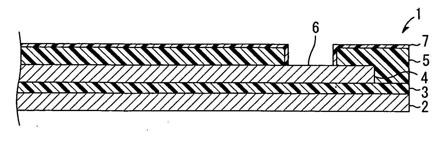
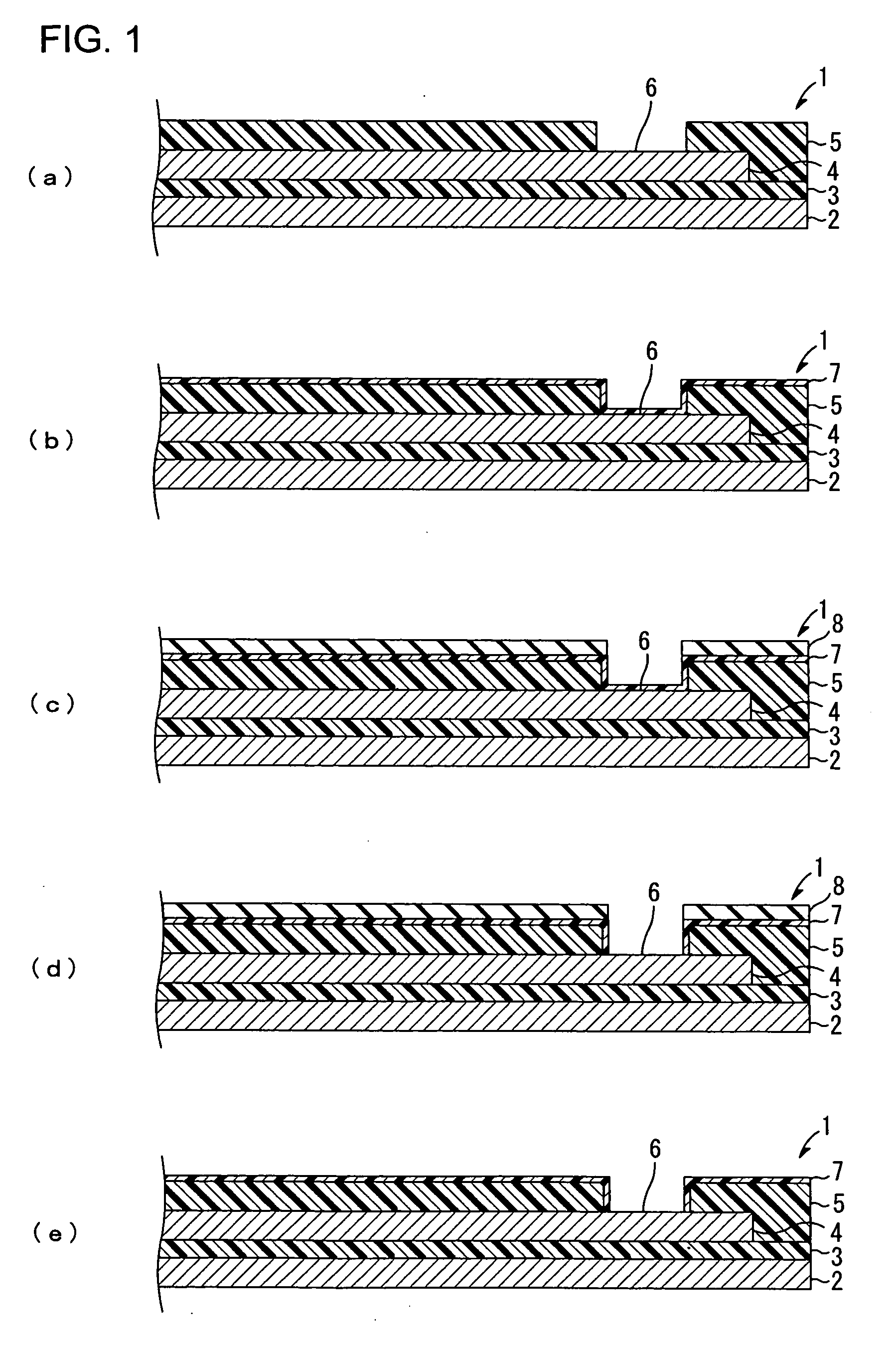
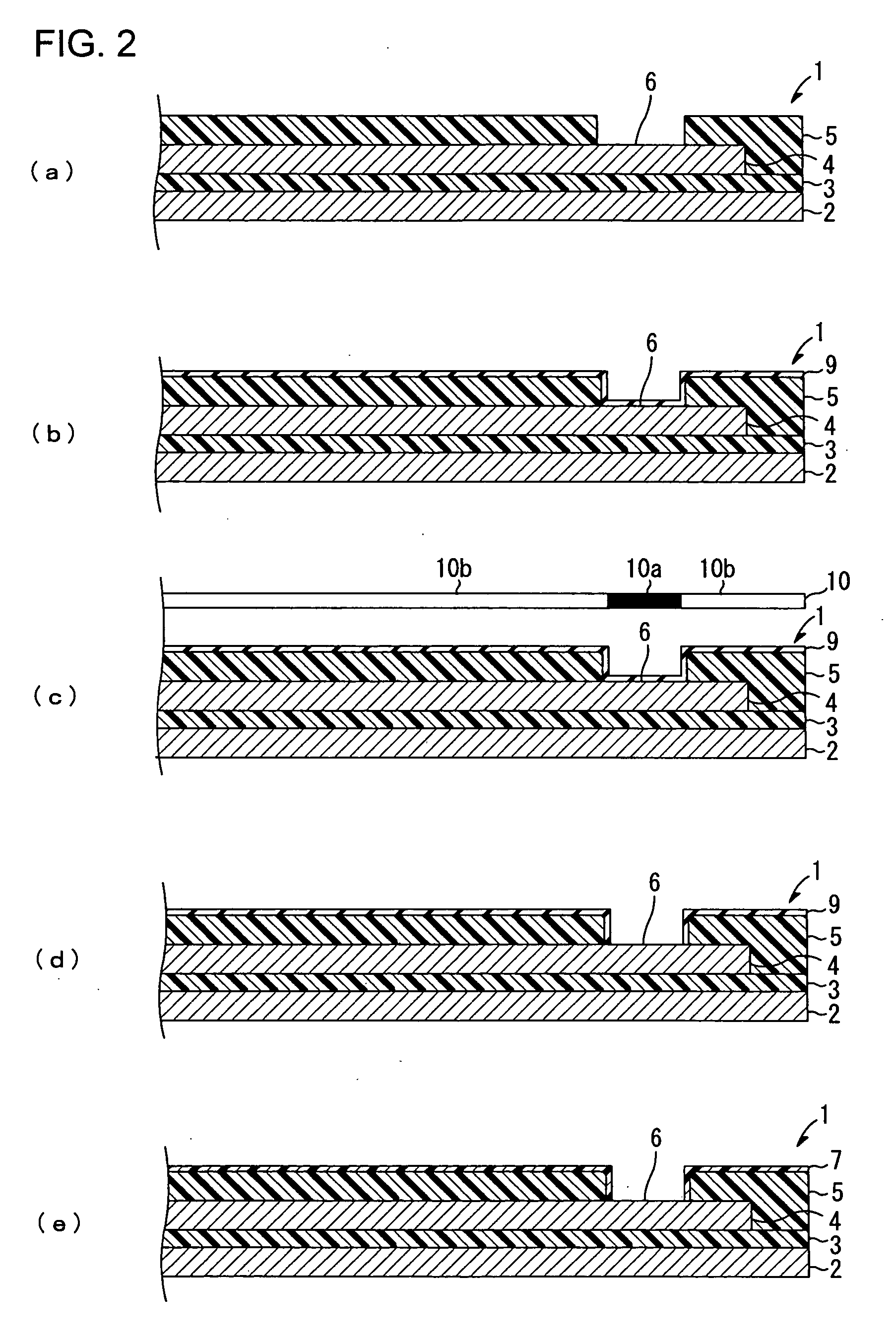
[0072] A suspension board with circuit was prepared by successively forming an insulating base layer composed of polyimide, a conductive pattern composed of copper foil, and an insulating cover layer composed of polyimide on a metal supporting board composed of stainless steel foil (see FIG. 1(a)). The opening was formed in the insulating cover layer so that the portion of the conductive pattern which was exposed through the opening serves as the terminal portion.

[0073] 15 g of a 10 wt % N-methyl-2-pyrrolidone (NMP) dispersion of carbon black (Special Black4™ commercially available from Degussa Japan, Ltd.) was added to 20 g of a 15 wt % NMP solution of polyether-imide (HR16NN™ commercially available from Toyobo. Co., Ltd.). The resulting mixture was stirred to provide a semi-conducting resin composition.

[0074] The semi-conducting resin composition was coated on the surface of the insulating cover layer including the terminal portion of the suspension board with circuit described ...

example 2

[0077] 22.3 g of a 19.9 wt % NMP dispersion of ITO particles (commercially available from Catalysts & Chemicals Industries Co., Ltd.) was added to 7 g of a 40 wt % NMP solution of polyether-imide (Ultem XH6050™ commercially available from GE Plastics Japan, Ltd.). The resulting mixture was stirred to provide a semi-conducting resin composition.

[0078] The semi-conducting resin composition was coated on the surface of the insulating cover layer including the terminal portion of a suspension board with circuit, which is the same as used in Example 1, by using a bar coater, dried at 100° C. for 5 minutes, and further dried at 180° C. for 15 minutes, thereby forming a semi-conducting layer with a thickness of 1 μm.

[0079] Subsequently, the same process steps as performed in Example 1 were performed, whereby the suspension board with circuit in which the semi-conducting layer was formed on the surface of the insulating cover layer except for that of the terminal portion was obtained.

[00...

example 3

[0081] 3.1 g of a 20.6 wt % NMP dispersion of PTO particles (commercially available from Catalysts & Chemicals Industries Co., Ltd.) was added to 2 g of a 15 wt % NMP solution of polyether-imide (HR16NN™ commercially available from Toyobo. Co., Ltd.). The resulting mixture was stirred to provide a solution of a semi-conducting resin composition.

[0082] The semi-conducting resin composition was coated on the surface of the insulating cover layer including the terminal portion of a suspension board with circuit, which is the same as used in Example 1, by using a bar coater, dried at 100° C. for 5 minutes, and further dried at 180° C. for 15 minutes, thereby forming a semi-conducting layer with a thickness of 2 μm.

[0083] Subsequently, the same process steps as performed in Example 1 were performed, whereby the suspension board with circuit in which the semi-conducting layer was formed on the surface of the insulating cover layer except for that of the terminal portion was obtained.

[0...


PUM

PropertyMeasurementUnit
Electrical conductoraaaaaaaaaa
Surface resistivityaaaaaaaaaa

Abstract

To provide a semi-conducting resin composition capable of forming a semi-conducting layer which exhibits a less variable surface resistivity even when subjected to ultrasonic cleaning and effectively discharges static electricity and also provide a wired circuit board comprising the semi-conducting layer composed of the semi-conducting resin composition, an imide resin or a precursor of an imide resin and conducting particles are mixed in a solvent so that the semi-conducting resin composition containing the imide resin or imide resin precursor dissolved therein and the conducting particles dispersed therein is prepared. Then, the semi-conducting resin composition is coated on a surface of an insulating cover layer (5) including the terminal portion (6) of a suspension board with circuit (1) and dried to form a semi-conducting layer (7). Thereafter, the semi-conducting layer 7 formed in the terminal portion (6) is removed by etching.

Description

CROSS REFERENCE TO RELATED APPLICATION [0001] This application claims priority from Japanese Patent Application No. 2005-011991, filed on Jan. 19, 2005 and Japanese Patent Application No. 2005-142815 filed on May 16, 2005, the contents of which are herein incorporated by reference in their entirety. BACKGROUND OF THE INVENTION [0002] 1. Field of the Invention [0003] The present invention relates to a semi-conducting resin composition and to a wired circuit board. More particularly, the present invention relates to a wired circuit board to be provided in electric / electronic equipment and to a semi-conducting resin composition for forming a semi-conducting layer in the wired circuit board. [0004] 2. Description of Related Art [0005] A wired circuit board, such as a flexible wired circuit board or a suspension board with circuit, typically comprises: a base layer composed of polyimide; a conductive circuit composed of copper foil formed on the base layer; and a cover layer composed of ...

Claims


Application Information

Patent Timeline
IPC IPC(8): C08F8/00B32B3/00
CPCC08L79/08H05K1/0259H05K1/056Y10T428/24917H05K2201/0154H05K2201/09554H05K1/167
Inventor UCHIYAMA, HISAEKINJOU, NAOTAKAKONDOU, TAKASHIFUKUOKA, TAKAHIROISHII, JUN
Owner NITTO DENKO CORP
Why Eureka
Try Eureka