Configuration for digital-analog conversion of high-frequency digital input signal into carrier-frequency analog output signal

a digital analog and carrier-frequency technology, applied in the field of digital analog conversion of high-frequency digital input signal into carrier-frequency analog output signal, can solve the problems of unwanted carrier frequency, large expense, replacement, etc., and achieve the effect of reducing the cost of filters, high quality, and easy suppression of quantization noise formed by converters on input signals

Inactive Publication Date: 2006-07-27
HMD GLOBAL
View PDF6 Cites 6 Cited by
  • Summary
  • Abstract
  • Description
  • Claims
  • Application Information

AI Technical Summary

Benefits of technology

[0015] A configuration according to the invention enables expenditure on filters to be considerably reduced, for any carrier frequency range, by prefiltering. Together with a corresponding power output stage, the elimination of the need for frequency-specific filtering at the transmitter end makes for high quality.
[0016] In particular, quantization noise formed by ΣΔ converters on the input signal can easily be suppressed by using a configuration according to the invention.
[0017] The filter function of a configuration according to the invention can be influenced by the signal form emitted by each D / A converter per datum or bit. By using a suitable signal form, such as—for example—multiple pulses, which consist of several pulses for each datum, the filter function can be improved selectively.

Problems solved by technology

These unwanted carrier frequencies can be caused, for example, by a less than perfect digital input signal or by various unwanted modulation mechanisms.
These must be replaced, at great expense, if a change in carrier frequency range is required.

Method used


Image

  • Configuration for digital-analog conversion of high-frequency digital input signal into carrier-frequency analog output signal
  • Configuration for digital-analog conversion of high-frequency digital input signal into carrier-frequency analog output signal
  • Configuration for digital-analog conversion of high-frequency digital input signal into carrier-frequency analog output signal

Examples


Embodiment Construction

[0021] Reference will now be made in detail to the preferred embodiments of the present invention, examples of which are illustrated in the accompanying drawings, wherein like reference numerals refer to like elements throughout.

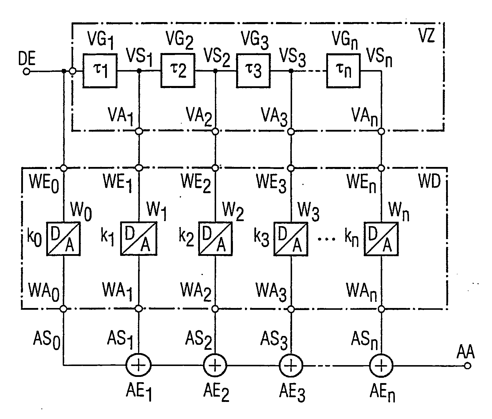
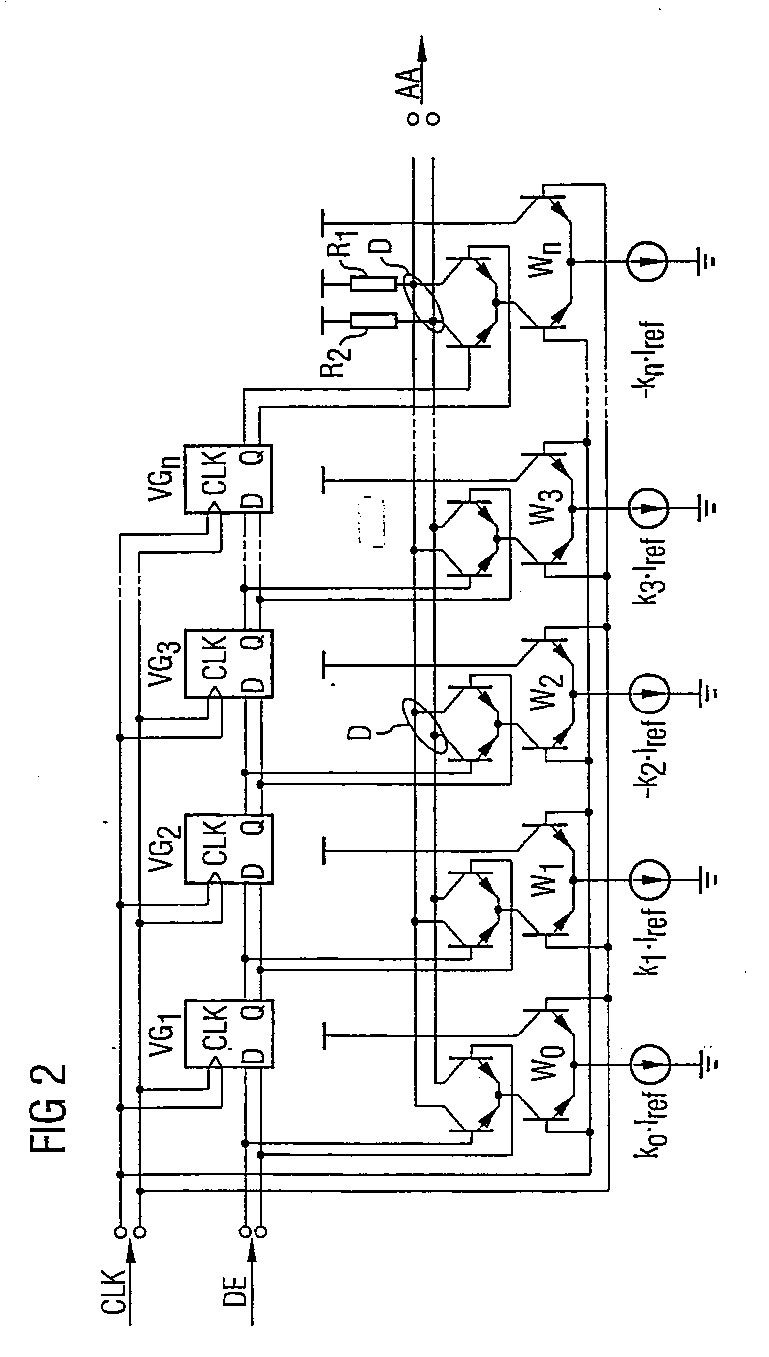
[0022]FIG. 1 shows a block diagram of a configuration for digital-analog conversion according to the invention.

[0023] A high-frequency digital input signal DE arrives at a delay device VZ and at a converter device WD.

[0024] The delay device VZ has n delay elements VG1, VG2, VG3, . . . , VGn, which are connected in a serially consecutive manner, and with a specific delay time τl, τ2, 963, . . . , τn being assigned to each of them. Each individual delay element VG1 to VGn is connected on the output side to an output VA1, VA2, VA3, . . . , VAn of the delay device VZ. Via each of these outputs VA1 to VAn, a delay signal VS1, VS2, VS3, . . . , VSn, assigned thereto in each case and formed by the corresponding delay element VG1 to VGn, reaches an input WE1, WE2...


PUM


Abstract

A delay device has at least one first delay element and optional additional delay elements connected downstream from the first in a serially consecutive manner. The digital input signal is connected to an input of the first delay element and is connected to an input of a first D/A converter. The output of the first delay element is connected to an input of another D/A converter assigned thereto. The optional additional delay elements each have outputs connected to an input of another D/A converter assigned to the respective delay elements. All D/A converters are combined on the output side in a step-by-step manner so that output signals of all D/A converters form the analog output signal or the device. A specific coefficient is assigned to each D/A converter, and a specific delay time is assigned to each delay element for realizing a filter characteristic.

Description

CROSS REFERENCE TO RELATED APPLICATIONS [0001] This application is based on and hereby claims priority to German Application No. 102 27 856.8 filed on 19 Aug. 2002 and European Application No. 02018602.9 filed on 19 Aug. 2002, the contents of which are hereby incorporated by reference. BACKGROUND OF THE INVENTION [0002] 1. Field of the Invention [0003] The invention relates to a configuration for the digital-analog conversion of a high-frequency digital input signal into a carrier-frequency analog output signal. [0004] 2. Description of the Related Art [0005] Architectures for the generation of a broadband, carrier-frequency output signal are known in which, in a low frequency range, a digital input signal is converted into an analog signal using a digital-analog converter, and then reconverted into the carrier-frequency output signal using one or more mixing stages. [0006] Furthermore, digital-analog converter architectures are known in which a carrier-frequency output signal is ge...

Claims


Application Information

Patent Timeline
Patent Type & Authority Applications(United States)
IPC IPC(8): H03M1/66H03M1/00H03M1/06H03M1/74H03M3/02
CPCH03M1/0626H03M1/66H03M1/74H03M3/396H03M3/41H03M3/504H03M1/00
Inventor FUCHS, ARMINJELONNEK, BJORNWOLFF, GUNTER
Owner HMD GLOBAL
Why Eureka
Try Eureka