Organic light emitting display device

a light-emitting display and organic technology, applied in the direction of discharge tube luminescnet screens, discharge tube/lamp details, manufacturing tools, etc., can solve the problems of increasing the product of current and resistance (ir) or the voltage drop, increasing the number of interconnection lines, and increasing the voltage drop. , to achieve the effect of reducing the dead space, expanding the display region, and reducing the voltage drop of the display devi

Active Publication Date: 2006-08-03
SAMSUNG DISPLAY CO LTD
View PDF6 Cites 25 Cited by
  • Summary
  • Abstract
  • Description
  • Claims
  • Application Information

AI Technical Summary

Benefits of technology

[0012] The present invention provides an organic light emitting display device or an organic light emitting diode (OLED) display de

Problems solved by technology

Further, as the OLED display device includes more varied and complicated functions, it needs more interconnection lines.
However, this method leads to an increase in volt

Method used


Image

  • Organic light emitting display device
  • Organic light emitting display device
  • Organic light emitting display device

Examples


first embodiment

[0052] The OLED display device of the present embodiment is similar to the OLED display device of the first embodiment except for the differences described in that foregoing paragraphs.

[0053]FIGS. 4A and 4B respectively illustrate a plan view of a substrate and a bottom view of an encapsulation substrate of an OLED display device according to a third exemplary embodiment of the present invention.

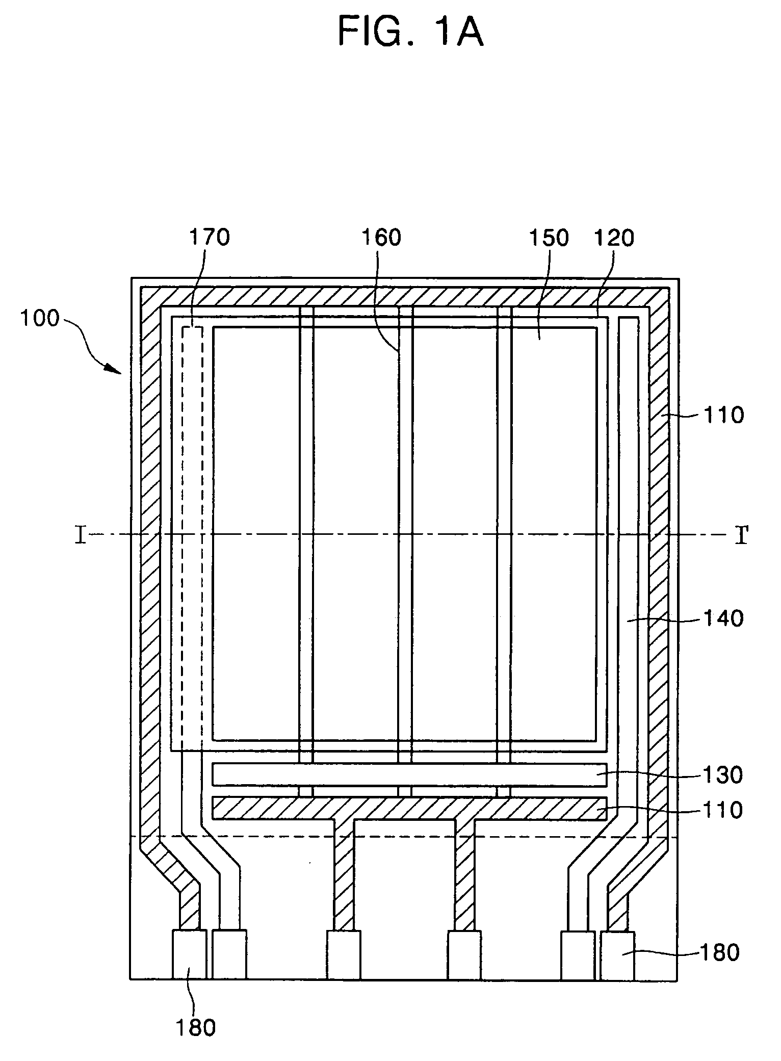
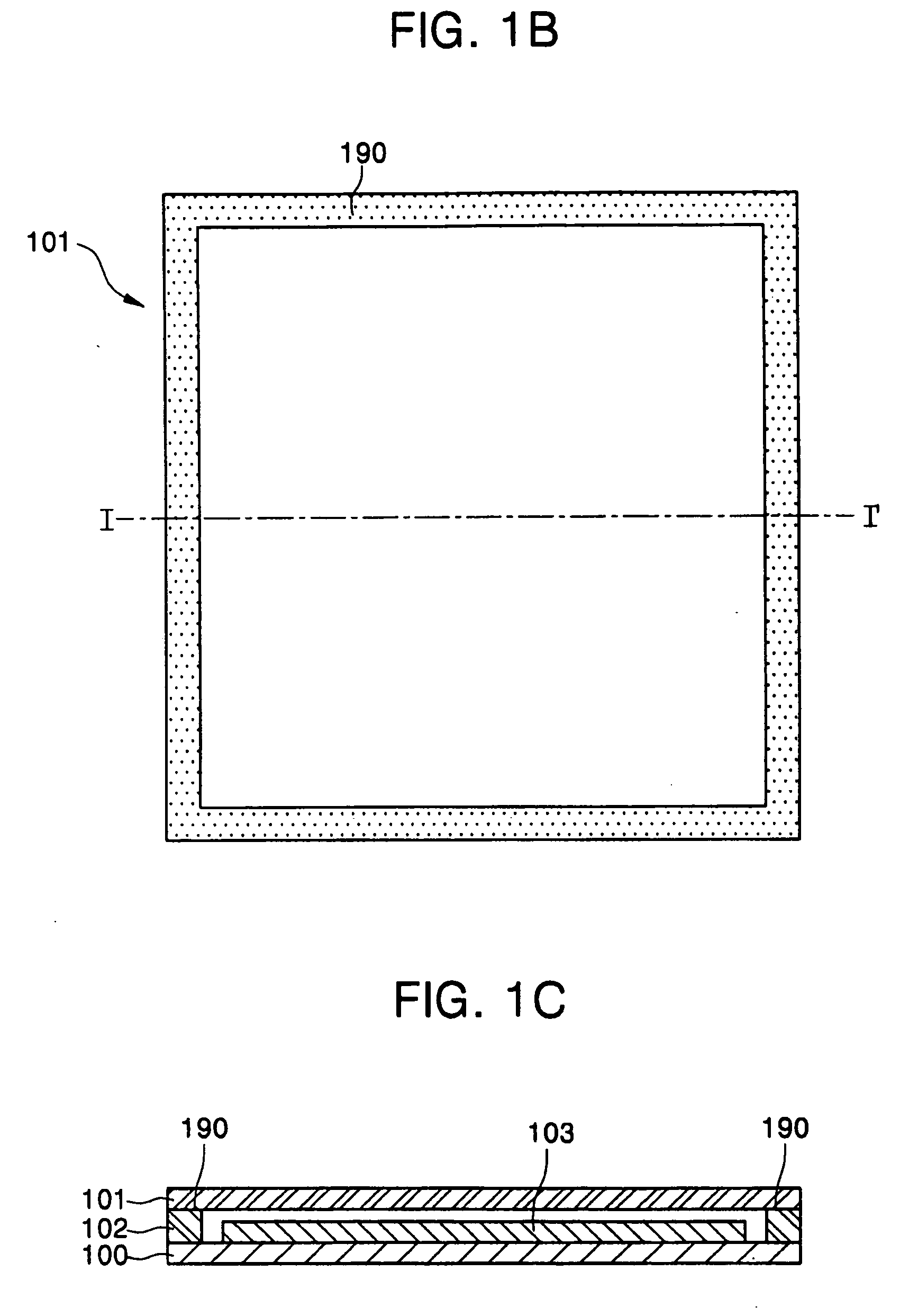
[0054] Referring to FIG. 4A, a display region 450 including predetermined pixels is disposed on a substrate 400. Common power lines 460, scan lines (not shown), and data lines (not shown) are disposed in the display region 450. The common power lines 460 are used to apply a voltage to the respective pixels. The scan lines are connected to a scan driver 140 that outputs selection signals, and the data lines are connected to a data driver 130 that outputs data signals.

[0055] The display region 450 may include an anode electrode (not shown), a cathode electrode 420, and a thin organic layer (...

fifth embodiment

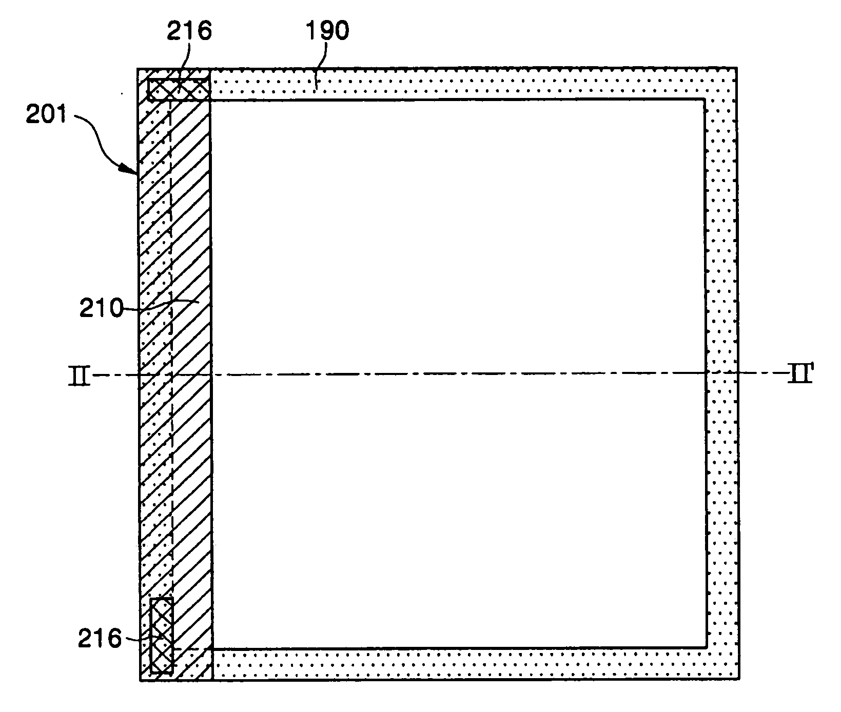
[0075] In the fifth embodiment, no cathode power supply line is disposed on the substrate 600. A cathode power supply line 670, shown in FIG. 6B, does not overlap the cathode electrode 620 but is disposed in a predetermined region of an encapsulation substrate 601 that will be described later. Thus, the display region 650 can be further expanded. That is, a space otherwise occupied by the cathode power supply line 670 can be used as the display region 650.

[0076]FIG. 6B shows a bottom surface of the encapsulation substrate 601.

[0077] The cathode power supply line 670 is disposed on a surface of the encapsulation substrate 601 opposite to the substrate 600. The cathode power supply line 670 is disposed on left and right sides of the encapsulation substrate 601. However, the present invention is not limited thereto but a sectional area of the cathode power supply line 670 may be enlarged to decrease line resistance and reduce voltage drop. Also, the cathode power supply line 670 is no...


PUM

PropertyMeasurementUnit
Poweraaaaaaaaaa
Electrical conductoraaaaaaaaaa
Electric potential / voltageaaaaaaaaaa

Abstract

Provided is an organic light emitting diode (OLED) display device including a substrate on a front side of the OLED display device that is coupled to an encapsulation substrate on the back side of the OLED display device. An interconnection line is disposed in a predetermined region of the encapsulation substrate corresponding to a portion of the substrate on which no interconnection lines are disposed. Alternatively, a common power supply line is disposed only on the encapsulation substrate. As a result, a dead space in a display region of the substrate can be reduced so that other lines can be disposed in an interconnection line region of the substrate, and the display region can be further expanded. Also, since a wide interconnection line can be disposed on the encapsulation substrate, line resistance is decreased and a voltage drop can be reduced.

Description

CROSS-REFERENCE TO RELATED APPLICATION [0001] This application claims priority to and the benefit of the Korean Patent Application No. 10-2005-0010271, filed Feb. 3, 2005, in the Korean Intellectual Property Office, the entire content of which is incorporated herein by reference. BACKGROUND OF THE INVENTION [0002] 1. Field of the Invention [0003] The present invention relates to an organic light emitting display device, and more particularly, to an organic light emitting display device in which interconnection lines are disposed in a predetermined region of an encapsulation substrate. [0004] 2. Description of the Related Art [0005] Among flat panel display devices (FPDs), the organic light emitting display device, or organic light emitting diode (OLED) display device, has attracted much attention as the next generation FPD. Because the OLED display device is a self-emissive display device, it has advantages of a wide viewing angle, a fast response time, and a high contrast, and can ...

Claims


Application Information

Patent Timeline
IPC IPC(8): H05B33/04H01L51/50
CPCH01L27/3276H01L27/3288H01L51/524H10K59/179H10K59/131B22D41/001H10K50/841
Inventor KIM, SUN-HWASHIN, BONG-JU
Owner SAMSUNG DISPLAY CO LTD
Why Eureka
Try Eureka