Method for analyzing critical defects in analog integrated circuits

a technology of critical defects and integrated circuits, applied in the direction of testing circuits, resistance/reactance/impedence, instruments, etc., can solve the problems of failure analysis, failure analysis may typically acquire more detailed failure information, and write testing

Active Publication Date: 2006-08-03
TEXAS INSTR INC
View PDF7 Cites 15 Cited by
  • Summary
  • Abstract
  • Description
  • Claims
  • Application Information

AI Technical Summary

Benefits of technology

[0007] To address the above-discussed deficiencies of the prior art, the present invention provides a method for analyzing critical defects in analog integrated circuits, and a system for accomplishing the same. The method for analyzing critical defects, among other possible steps, may include fault testing a power field effect transistor portion of an analog integrated circuit to obtain electrical failure data. The method may further include performing an in-line optical inspection of the analog integrated circuit to obtain physical defect data, and correlating the electrical failure data and physical defect data to analyze critical defects.
[0008] As previously mentioned, the present invention further includes a system for analyzing critical defects in analog integrated circuits. Among other elements, the system includes: 1) a fault testing subsystem configured to test a power field effect transistor portion of an analog integrated circuit to obtain electrical failure data, 2) an optical inspection subsystem configured to perform an in-line optical inspection of the analog integrated circuit to obtain physical defect data, and 3) a correlation subsystem configured to correlate the electrical failure data and physical defect data to analyze critical defects.

Problems solved by technology

Apart from production testing is failure analysis.
Failure analysis attempts to identify the cause of failures of chips of a particular chip design after those failures have been detected during production (or prototype) testing.
Failure analysis may typically acquire more detailed failure information than that provided using the production (or prototype) testing.
Errors in read / write testing may be pinpointed as likely physical defects at readily identifiable locations on the chip.
Unfortunately, analog devices have little or no memory cells to accurately discern defect origins like their digital and memory device counterparts.
Moreover, running test chips is expensive and takes away from resources that might be used to make production chips.

Method used


Image

  • Method for analyzing critical defects in analog integrated circuits
  • Method for analyzing critical defects in analog integrated circuits
  • Method for analyzing critical defects in analog integrated circuits

Examples


Embodiment Construction

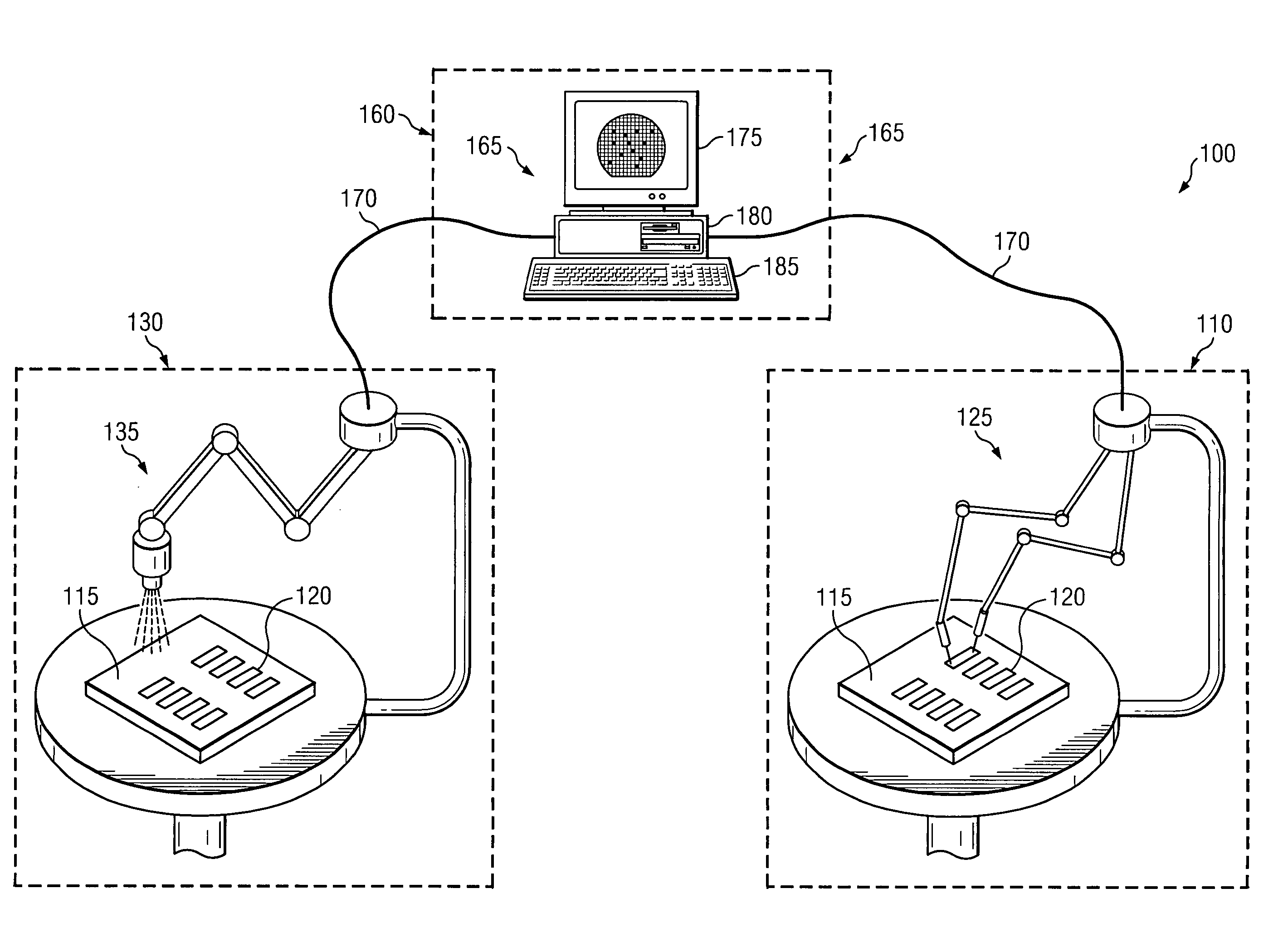
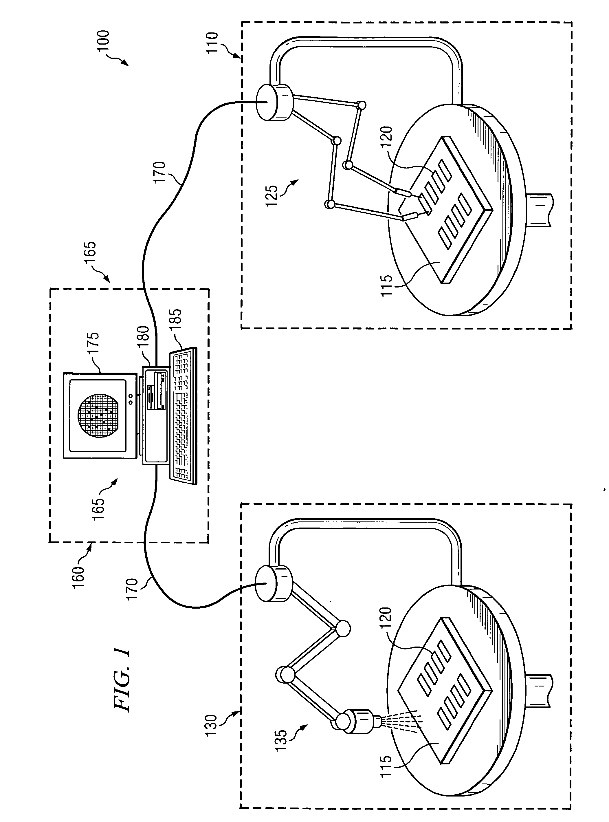
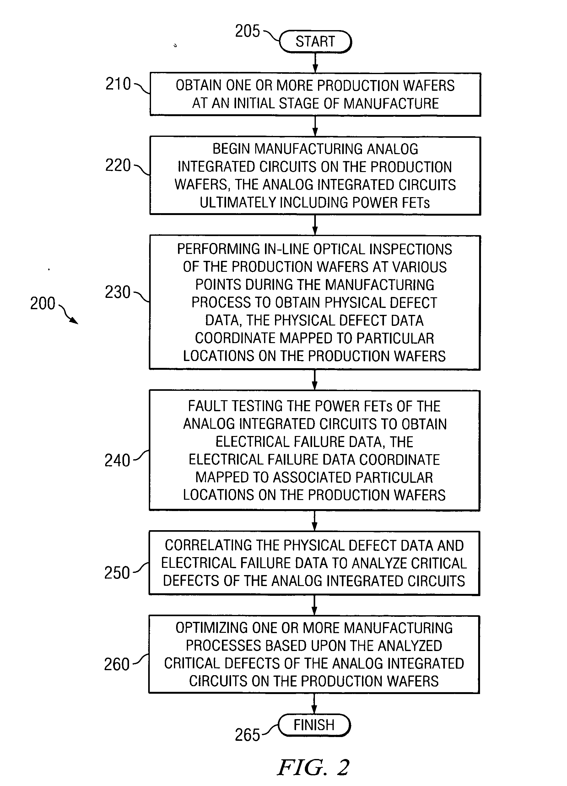
[0015] The present invention is based at least in part on the unique acknowledgement that analog based integrated circuits, and particularly their physical and electrical layout, are amenable to product wafer critical defect analysis thereof. Critical defect analysis, as referred to herein, is intended to encompass the process of discerning defects that cause a circuit to fail from defects that do not cause a circuit to fail. Heretofore, the semiconductor industry was unaware of the ability to conduct product wafer critical defect analysis testing on analog based integrated circuits, and thus relied upon test chip critical defect testing. The present invention has recognized, however, that the physical and electrical layout of the power field effect transistor (power FET) portion of the analog integrated circuits lends itself to a pass / fail fault analysis of the individual power FETs. This fault analysis may then, after a number of different optional and required processing steps, b...


PUM


Abstract

The present invention provides a method for analyzing critical defects in analog integrated circuits. The method for analyzing critical defects, among other possible steps, may include fault testing a power field effect transistor (120) portion of an analog integrated circuit (115) to obtain electrical failure data. The method may further include performing an in-line optical inspection of the analog integrated circuit (115) to obtain physical defect data, and correlating the electrical failure data and physical defect data to analyze critical defects.

Description

TECHNICAL FIELD OF THE INVENTION [0001] The present invention is directed, in general, to a method for testing integrated circuits and, more specifically, to a method for detecting critical defects in analog integrated circuits. BACKGROUND OF THE INVENTION [0002] Semiconductor chips may be divided into a number of different discrete categories, analog, digital, and memory devices, depending on the characterization. To accommodate the increasingly stringent requirements of today's semiconductor industry, analog, digital and memory devices often require production monitoring and testing. Production monitoring is typically performed using “in-line” inspection equipment, and production testing is performed using “end-of-line” test equipment. In-line inspection equipment often inspects entire semiconductor wafers, each of which may have formed thereon hundreds of chips. End-of-line test equipment performs “electrical testing” on semiconductor wafers in which the pads of chips are contact...

Claims


Application Information

Patent Timeline
Patent Type & Authority Applications(United States)
IPC IPC(8): G11C29/00
CPCG01R31/2894G01R31/311
Inventor MOLLAT, MARTIN B.KHANDEKAR, MILIND V.PHAN, TONY T.FLESSNER, KYLE M.
Owner TEXAS INSTR INC
Why Eureka
Try Eureka