Inspection method and its apparatus, inspection system

a technology of inspection method and inspection system, applied in the field of inspection, can solve the problems of difficult to improve a yield effectively, not efficiently reviewing the necessary defect, not being taken by priority, etc., and achieve the effect of improving the efficiency of inspection

Inactive Publication Date: 2005-02-10
HITACHI LTD
View PDF21 Cites 22 Cited by
  • Summary
  • Abstract
  • Description
  • Claims
  • Application Information

AI Technical Summary

Benefits of technology

[0009] The present invention provides an inspection method that can judge a defect which should be reviewed by priority so as to improve efficiency in inspection, and also provides a tool therefor.
[0010] Further, the present invention provides a manufacturing method of a semiconductor device that can take measures against a failure efficiently to improve a yield of the semiconductor device by judging a defect which should be reviewed by priority so as to improve efficiency in inspection.
[0019] This permits a defect which has a high possibility of influencing a yield to be efficiently reviewed by priority, whereby a direct factor exerting the influence can be identified in a short period of time and measures against the factor can easily be taken. Consequently, time taken to produce a defective unit is shortened, which leads to improvement in yield.

Problems solved by technology

Although it was possible to grasp statistically a tendency of defects using the conventional random sampling, a necessary defect was not efficiently reviewed.
For example, measures could not be taken by priority against a critical defect causing an electrical failure; with the result that it was difficult to improve a yield effectively.
For this reason, performance of the inspection tool is being enhanced accordingly, leading to an increase in the number of defects to be detected.

Method used


Image

  • Inspection method and its apparatus, inspection system
  • Inspection method and its apparatus, inspection system
  • Inspection method and its apparatus, inspection system

Examples


Embodiment Construction

[0042] Preferred embodiments of a method for inspecting a semiconductor device and its tool, and preferred embodiments of a method for manufacturing the semiconductor device, according to the present invention, will be described below with reference to the drawing.

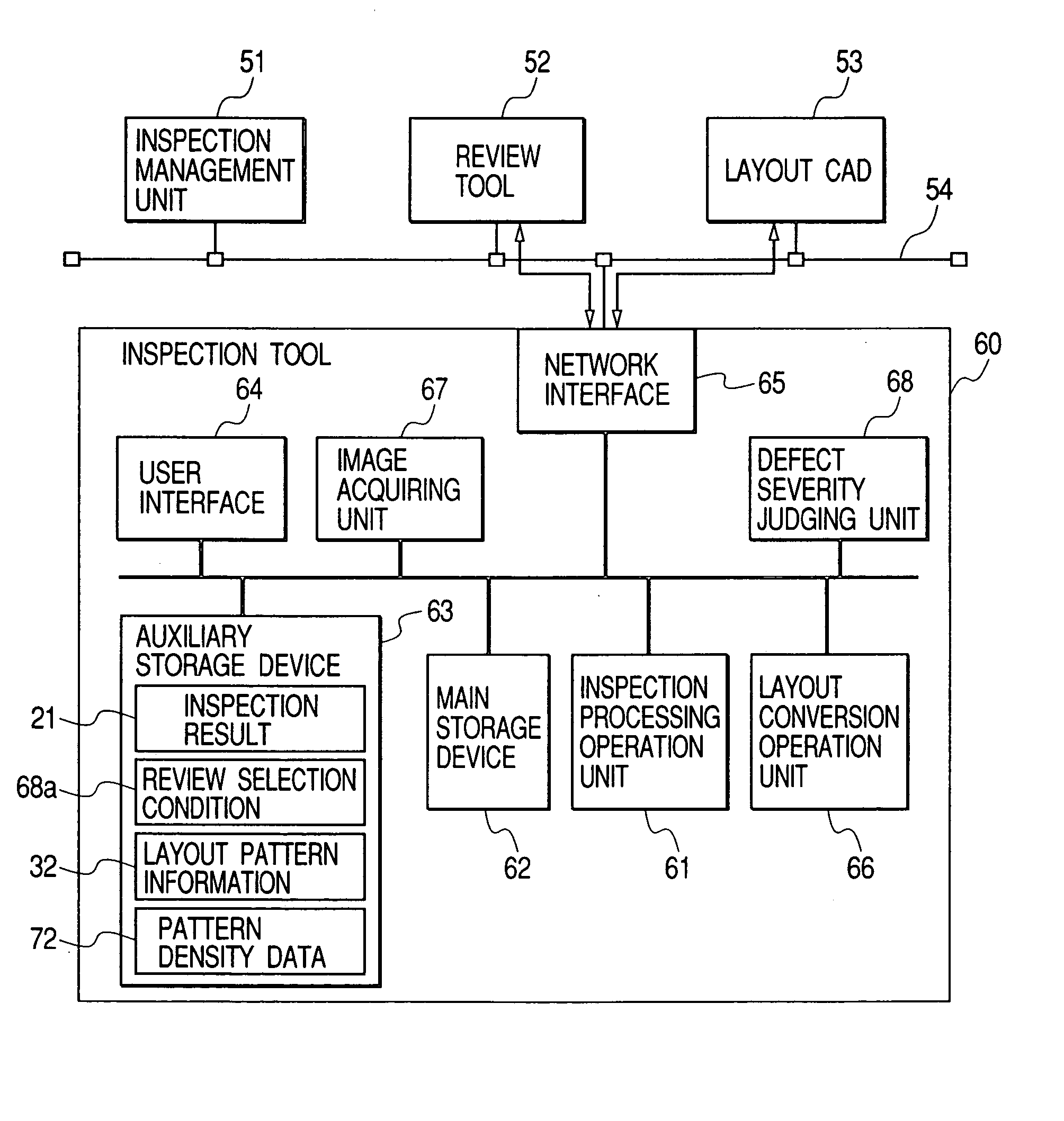
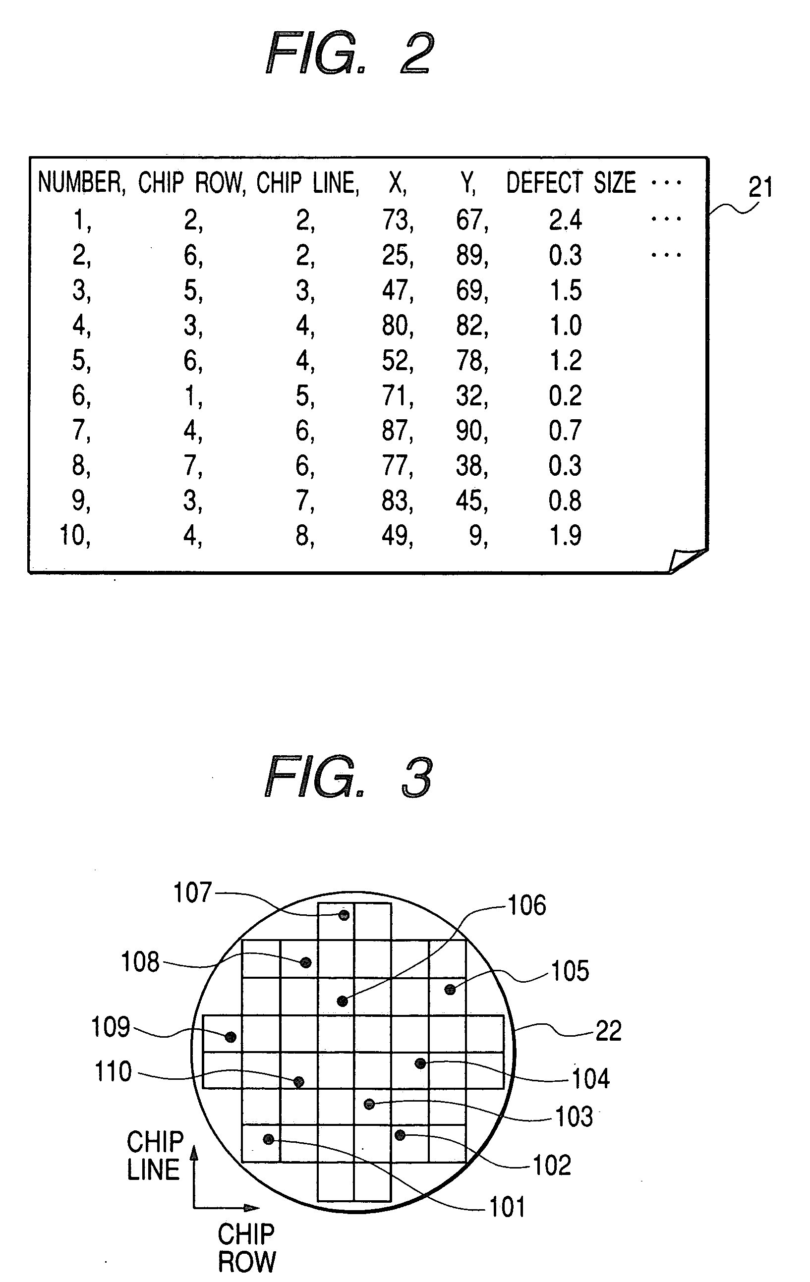
[0043]FIG. 9 illustrates a distribution map 36 showing how positions of defects detected by an inspection-processing unit 61 of an inspection tool 60 in a configuration shown in FIG. 1 are distributed in a chip. This distribution map 36 showing the defect positions distributed in the chip is made by plotting data 35 of the detected defects on a schematic diagram 32 illustrating a circuit layout of a LSI chip. To be more specific, the detected defects are plotted according to position coordinates in respective LSI chips on a wafer. Each black dot indicates an individual defect. Rectangular frames B1 through B7 indicate positions of LSI function block 1 through LSI function block 7, respectively. Here, the LSI function bloc...


PUM

PropertyMeasurementUnit
angleaaaaaaaaaa
sizeaaaaaaaaaa
defectsaaaaaaaaaa

Abstract

The present invention relates to a tool for analyzing by priority a defect having a high possibility of causing an electrical failure when inspecting a particle and a pattern defect in a piece of work which constitutes an electronic device such as a semiconductor integrated circuit, and relates to a system therefor. On the basis of the result of comparison between defect information which is the result of inspection by an inspection tool and layout data stored in an auxiliary storage device, or on the basis of the result of reinspection by comparison between a defect and a wiring pattern as a background by an inspection processing operation unit, an object to be reviewed is selected using review conditions stored in the auxiliary storage device.

Description

BACKGROUND OF THE INVENTION [0001] The present invention relates to an inspection method used in a production process of an electronic device such as a semiconductor integrated circuit, and relates to an inspection apparatus or inspection tool and an inspection system, which are used for realizing the inspection method, and a manufacturing method of a semiconductor device. [0002] In the production of an electronic device typified by a semiconductor integrated circuit, after a defect is detected by darkfield and brightfield inspection tools, the detected defect is often reviewed in order to analyze an individual detected defect using a defect review function provided in the inspection tool itself or a dedicated image acquiring tool, such as a review apparatus or review tool, having an electron microscope, etc. [0003] It is to be noted that the darkfield inspection tool detects a particle adhered to a wafer whereas the brightfield inspection tool detects a particle and a pattern defec...

Claims


Application Information

Patent Timeline
Patent Type & Authority Applications(United States)
IPC IPC(8): G01N21/956G01B11/30H01L21/66
CPCG01N21/95607
Inventor OKABE, TAKAFUMIMAEDA, SHUNJISAKAI, KAORU
Owner HITACHI LTD
Why Eureka
Try Eureka