Manufacturing method of semiconductor device

a manufacturing method and semiconductor technology, applied in semiconductor devices, semiconductor/solid-state device details, electrical devices, etc., can solve the problems of weak pressure applied from both sides, chip cracking, and lowering the production yield of the semiconductor device which is in the form of a resin sealed semiconductor package, so as to improve the heat dissipation characteristic of the semiconductor device and improve the production yield of the semiconductor devi

Inactive Publication Date: 2006-08-10
RENESAS ELECTRONICS CORP
View PDF6 Cites 18 Cited by
  • Summary
  • Abstract
  • Description
  • Claims
  • Application Information

AI Technical Summary

Benefits of technology

[0024] It is possible to improve the production yield of the semiconductor device.
[0025] It is possible to improve the heat dissipating characteristic of the semiconductor device.

Problems solved by technology

However, when the mold is clamped in the molding process in such a manner that the terminals on the upper side of the semiconductor chip come into contact with the upper mold half and the terminals on the lower side of the semiconductor chip come into contact with the lower mold half, if the height of the assembly concerned varies just before the molding process or if the parallelism between the upper and lower terminals of the semiconductor chip varies, it is likely that strong pressures may be applied from both upper and lower mold halves, i.e., from both above and below, to the semiconductor chip through both upper and lower terminals of the semiconductor chip.
Once pressures are applied from above and below to the semiconductor chip, there is a fear that the semiconductor chip may be cracked, with consequent lowering of the production yield of the semiconductor device which is in the form of a resin sealed semiconductor package.

Method used


Image

  • Manufacturing method of semiconductor device
  • Manufacturing method of semiconductor device
  • Manufacturing method of semiconductor device

Examples


first embodiment

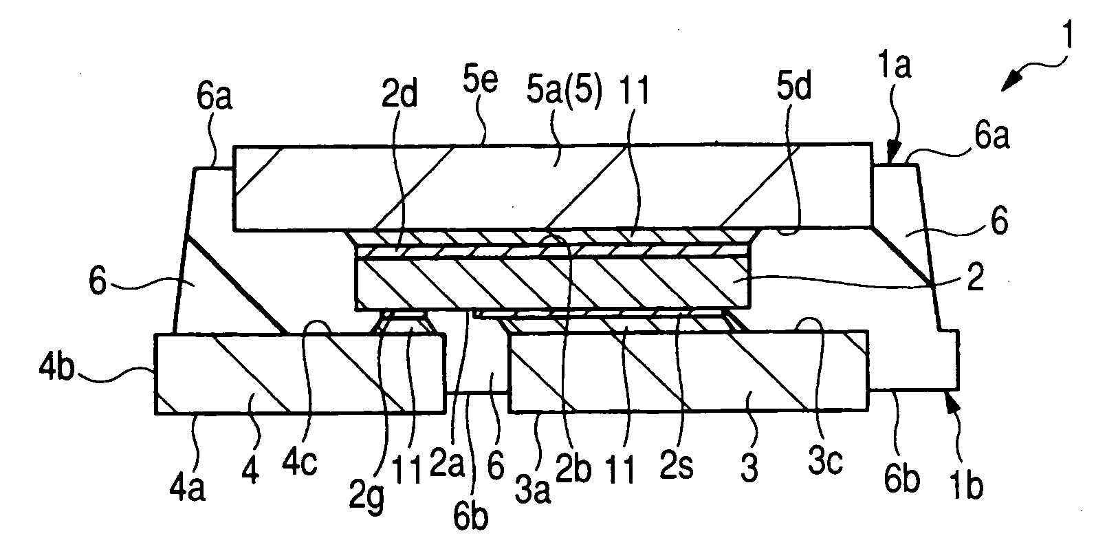
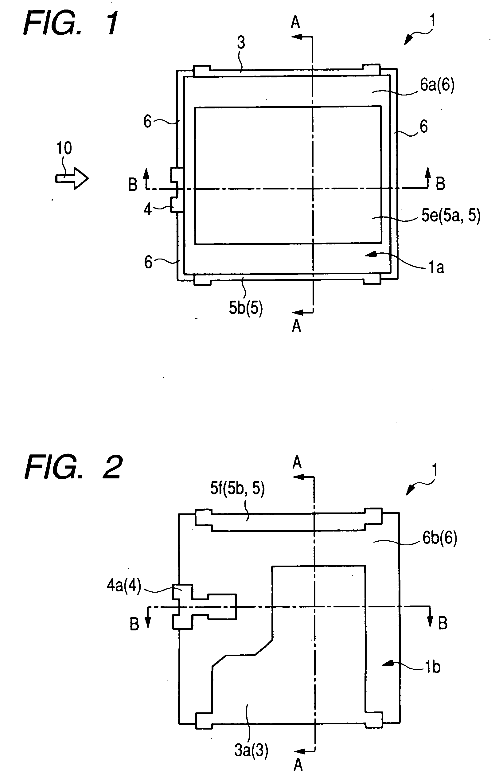
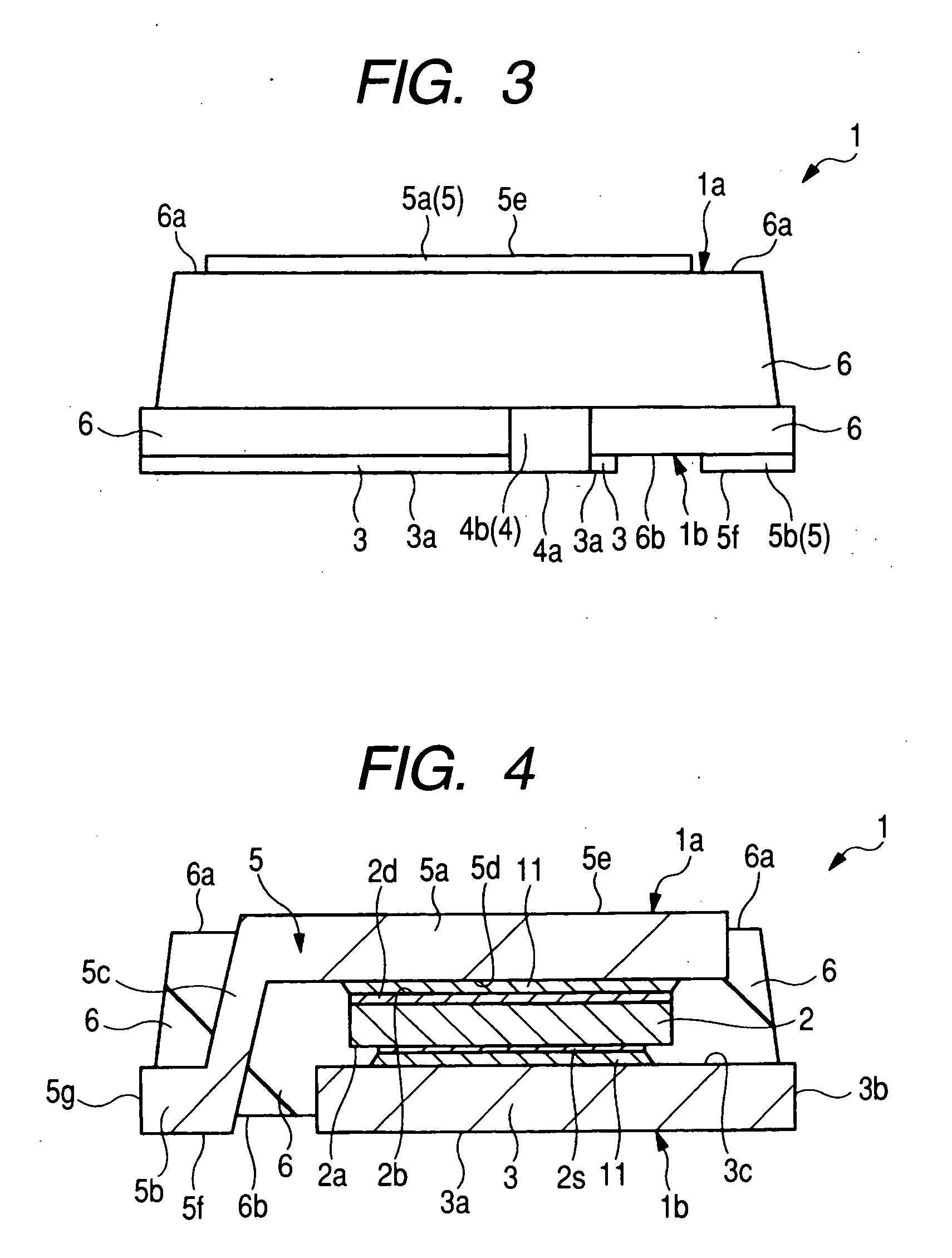
[0074] A semiconductor device according to a first embodiment of the present invention will be described below with reference to drawings.

[0075]FIG. 1 is a top view (plan view) of a semiconductor device 1 according to an embodiment of the present invention, FIG. 2 is a bottom view (back view or plan view) thereof, FIG. 3 is a side view thereof, and FIGS. 4 and 5 are sectional views (sectional side views) thereof. A section taken on line A-A in FIG. 1 (i.e., a section taken on line A-A in FIG. 2) corresponds approximately to FIG. 4 and a section taken on line B-B in FIG. 1 (i.e., a section taken on line B-B in FIG. 2) corresponds approximately to FIG. 5. FIG. 3 corresponds approximately to a side view of the semiconductor device 1 as seen in the direction of arrow 10 in FIG. 1.

[0076] The semiconductor device (semiconductor package) 1 of this embodiment is a resin sealed, surface mounting type semiconductor package. That is, the semiconductor device 1 is in the form of a resin seale...

second embodiment

[0157] In the previous first embodiment the polishing process of step S6 for the sealing resin portion 26 is carried out by liquid honing, but in this second embodiment the polishing process of step S6 for the sealing resin portion 26 is carried out by mechanical polishing. This second embodiment is almost the same as the first embodiment except that the polishing process of step S6 for the sealing resin portion 26 is performed by mechanical polishing instead of liquid polishing. Therefore, a description will be omitted as to the portion common to the first embodiment.

[0158]FIG. 33 is an explanatory diagram of the polishing process of step S6 for the sealing resin portion 26 according to this embodiment and FIG. 34 is a sectional view (a sectional view of a principal portion) showing a state after polishing of the sealing resin portion 26, corresponding to FIG. 26 or FIG. 28 in the first embodiment.

[0159] In this embodiment, after forming the sealing resin portion 26 by carrying o...

third embodiment

[0164] The polishing process of step S6 for the sealing resin portion 26 in the first embodiment is carried out by liquid honing, while in this third embodiment the polishing process of step S6 for the sealing resin portion 26 is performed by a combination of both mechanical polishing and liquid polishing. Other constructional points are about the same as in the first embodiment and therefore a description thereof will here be omitted.

[0165] FIGS. 35 to 38 are explanatory of the polishing process of step S6 for the sealing resin portion 26 in this third embodiment.

[0166] In this third embodiment, after forming the sealing resin portion 26 in step S5 in the same way as in the first embodiment, first the upper surface 26a side of the sealing resin portion 26 is polished by mechanical polishing. For example, as shown schematically in FIG. 35, the assembly (work) 40 which has been formed with the sealing resin portion 26 in step S5 is placed on the conveyance lane or table 60 and the ...


PUM


Abstract

A semiconductor device in the form of a resin sealed semiconductor package is disclosed, wherein a gate terminal connected to a gate pad electrode formed on a surface of a semiconductor chip and a source terminal connected to a source pad electrode formed on the chip surface exposed to a back surface of a sealing resin portion, a first portion of a drain terminal connected to a back-surface drain electrode of the semiconductor chip is exposed to an upper surface of the sealing resin portion, and a second portion of the drain terminal formed integrally with the first portion of the drain terminal is exposed to the back surface of the sealing resin portion. When forming the sealing resin portion in such a semiconductor device, first the sealing resin portion is formed so as to also cover an upper surface of the first portion of the drain terminal and thereafter the upper surface side of the sealing resin portion is polished by liquid honing, thereby allowing the upper surface of the first portion of the drain terminal to be exposed on the upper surface of the sealing resin portion. Both heat dissipating property and production yield of the semiconductor device are improved.

Description

CROSS-REFERENCE TO RELATED APPLICATION [0001] The present application claims priority from Japanese patent application No. 2005-031597 filed on Feb. 8, 2005, the content of which is hereby incorporated by reference into this application. BACKGROUND OF THE INVENTION [0002] The present invention relates to a method of manufacturing a semiconductor device and more particularly to a technique applicable effectively to the manufacture of a semiconductor device which is in the form of a resin sealed semiconductor package. [0003] Various semiconductor packages are in use, among which there is known a resin sealed semiconductor package including a semiconductor chip sealed with a resin sealing portion. In the resin sealed semiconductor package, a semiconductor chip is sealed within the resin sealing portion, so that the reliability of the semiconductor chip can be improved. Besides, by exposing terminals on a back surface of the resin sealing portion it becomes possible to effect surface-mo...

Claims


Application Information

Patent Timeline
Patent Type & Authority Applications(United States)
IPC IPC(8): H01L21/50
CPCH01L23/3107H01L23/49537H01L2924/1306H01L23/49562H01L24/36H01L24/40H01L24/41H01L24/84H01L2924/01002H01L2924/01005H01L2924/01013H01L2924/01015H01L2924/01029H01L2924/01051H01L2924/01074H01L2924/01078H01L2924/01079H01L2924/01082H01L2924/14H01L2924/01006H01L2924/01033H01L2924/01047H01L2924/01067H01L2924/014H01L2224/32245H01L2924/00H01L2924/351H01L2924/181H01L2224/84801H01L2224/37147H01L2224/83801H01L2224/8385H01L2224/8485H01L24/37H01L2224/371H01L2924/00012H01L2924/00014
Inventor MUTO, AKIRASHIMIZU, ICHIOARAI, KATSUOKAGII, HIDEMASASATO, HIROSHINAKAMURA, HIROYUKINAKAJO, TAKUYAOKAWA, KEIICHIOSAKA, MASAHIKO
Owner RENESAS ELECTRONICS CORP
Why Eureka
Try Eureka