Eureka AIR delivers breakthrough ideas for toughest innovation challenges, trusted by R&D personnel around the world.

Method of forming chip-type low-k dielectric layer

Inactive Publication Date: 2006-08-17
TOUCH MICRO SYST TECH
View PDF6 Cites 8 Cited by
  • Summary
  • Abstract
  • Description
  • Claims
  • Application Information

AI Technical Summary

Benefits of technology

[0022] The present invention utilizes a photosensitive material as the dielectric layer, and thus openings with an outwardly-inclined sidewall can be directly formed by an exposure-and-development process. Consequently, a diffusion barrier layer and a seed layer formed successively have an excellent step coverage effect. This ensures excellent electrical performance of the planar inductor components to be fabricated.

Problems solved by technology

However, several drawbacks come with the conventional method.
First, it is not very easy to control the etching selection ratio of the photoresist pattern 18 to dielectric layer 16, and thus defects tend to appear in the upper portion of the opening 20.
As long as the shape and the surface characteristic of the dielectric layer openings is degraded, the electrical performance of solder bumps or planar inductor components to be formed successively is seriously affected.

Method used


Image

  • Method of forming chip-type low-k dielectric layer
  • Method of forming chip-type low-k dielectric layer
  • Method of forming chip-type low-k dielectric layer

Examples


Embodiment Construction

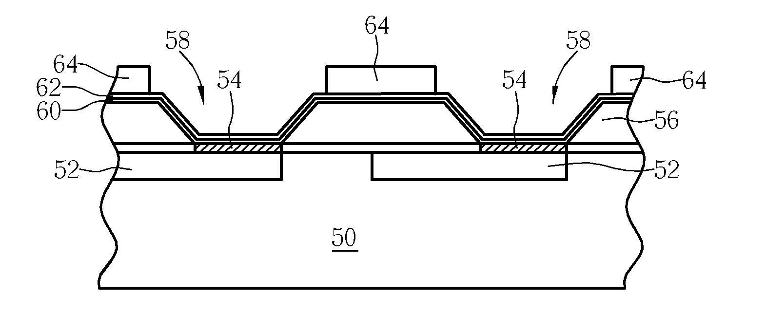
[0027] Please refer to FIG. 5 through FIG. 7. FIG. 5 through FIG. 7 are schematic diagrams illustrating a method of forming a chip-type low-k dielectric layer according to a preferred embodiment of the present invention. As shown in FIG. 5, a substrate 50, for instance a semiconductor substrate, is provided. The substrate 50 includes a plurality of semiconductor devices 52, and a plurality of contact pads 54, for instance metal bonding pads, electrically connected to the semiconductor devices 52. As shown in FIG. 6, a photosensitive dielectric layer 56 is formed on the surface of the substrate 50. The photosensitive dielectric layer 56 covers both the substrate 50 and the contact pads 54. Here, the photosensitive dielectric layer 56 is not only dielectric, but also can be patterned by an exposure-and-development process. In this embodiment, the material of the photosensitive dielectric layer 56 is selected from, but not limited to, photosensitive benzocyclobutene (BCB) or low-k poly...


PUM


Abstract

A substrate including a plurality of contact pads is provided. Thereafter, a photosensitive dielectric layer is formed on a surface of the substrate. Subsequently, an exposure-and-development process is preformed to partially remove the photosensitive dielectric layer so as to form a plurality of openings. The openings at least expose the contact pads, and the sidewall of each opening is inclined outwardly.

Description

BACKGROUND OF INVENTION [0001] 1. Field of the Invention[0002] The present invention relates to a method of forming a chip-type low-k dielectric layer, and more particularly, to a method of forming openings with an outwardly-inclined sidewall in a photosensitive dielectric layer, so as to form planar inductor components. [0003] 2. Description of the Prior Art [0004] In the fabrication of semiconductor devices, a dielectric layer mainly plays the role of providing an insulating effect. While selecting a suitable dielectric layer, parameters, such as the dielectric constant (k value) and the stress between the dielectric layer and other materials that contact with the dielectric layer, must be considered. In addition, openings are normally formed in the dielectric layer for forming solder bumps or other passive components. For some passive components, particularly planar inductor components, the shape and surface characteristic of the dielectric layer openings are critical to the elec...

Claims


Application Information

Patent Timeline
IPC IPC(8): H01L21/44H01L21/20
CPCH01L21/312H01L21/76804H01L23/5227H01L23/5283H01L23/53238H01L23/53252H01L24/11H01L2224/13099H01L2924/01022H01L2924/01029H01L2924/01073H01L2924/01074H01L2924/01078H01L2924/01079H01L2924/04941H01L2924/04953H01L2924/19042H01L2924/01005H01L2924/01006H01L2924/01019H01L2924/01033H01L2924/014H01L2224/05027H01L2224/05026H01L2224/05001H01L2224/05572H01L2224/05166H01L2224/05181H01L2224/05184H01L2224/05644H01L2224/05647H01L21/02118H01L24/03H01L2924/00014H01L21/02362
Inventor HU, SHU-HUAHUANG, KUAN-JUIPAN, CHIN-CHANGHUANG, SHIH-MIN
Owner TOUCH MICRO SYST TECH
Why Eureka
Eureka Blog
Learn More