Ceramic electronic component and multilayer capacitor

Active Publication Date: 2006-08-24
TDK CORPARATION
View PDF7 Cites 18 Cited by
  • Summary
  • Abstract
  • Description
  • Claims
  • Application Information

AI Technical Summary

Benefits of technology

[0007] In the external electrodes of the ceramic electronic component disclosed in Patent Document 2, an electrode layer of a base metal such as Ni, Cu, Sn, or Sn—Pb is formed immediately below the resin layer. For this reason, if the resin layer absorbs water, the surface of the electrode layer of the base metal immediately below the resin layer will oxidize, so as to increase the electric resistance of the ceramic electronic component.
[0018] The present invention successfully provides the ceramic electronic component and multilayer capacitor capable of realizing the reduction of cost, preventing the occurrence of the crack due to the thermal shock, and suppressing the increase in the electric resistance.

Problems solved by technology

Therefore, in cases where the internal electrodes are made of a base metal such as Ni in order to reduce cost, mechanical strength is not enough between the external electrodes and the ceramic sintered body, so that the external electrodes could peel off the ceramic sintered body.
For this reason, where the internal electrodes are made of a base metal, a problem will arise in either of cases where the electrode layer below the resin layer is a layer of a base metal or a layer of a noble metal.

Method used


Image

  • Ceramic electronic component and multilayer capacitor
  • Ceramic electronic component and multilayer capacitor

Examples


Embodiment Construction

[0022] A preferred embodiment of the present invention will be described below in detail with reference to the accompanying drawing. In the description, identical elements or elements with identical functionality will be denoted by the same reference symbols, without redundant description.

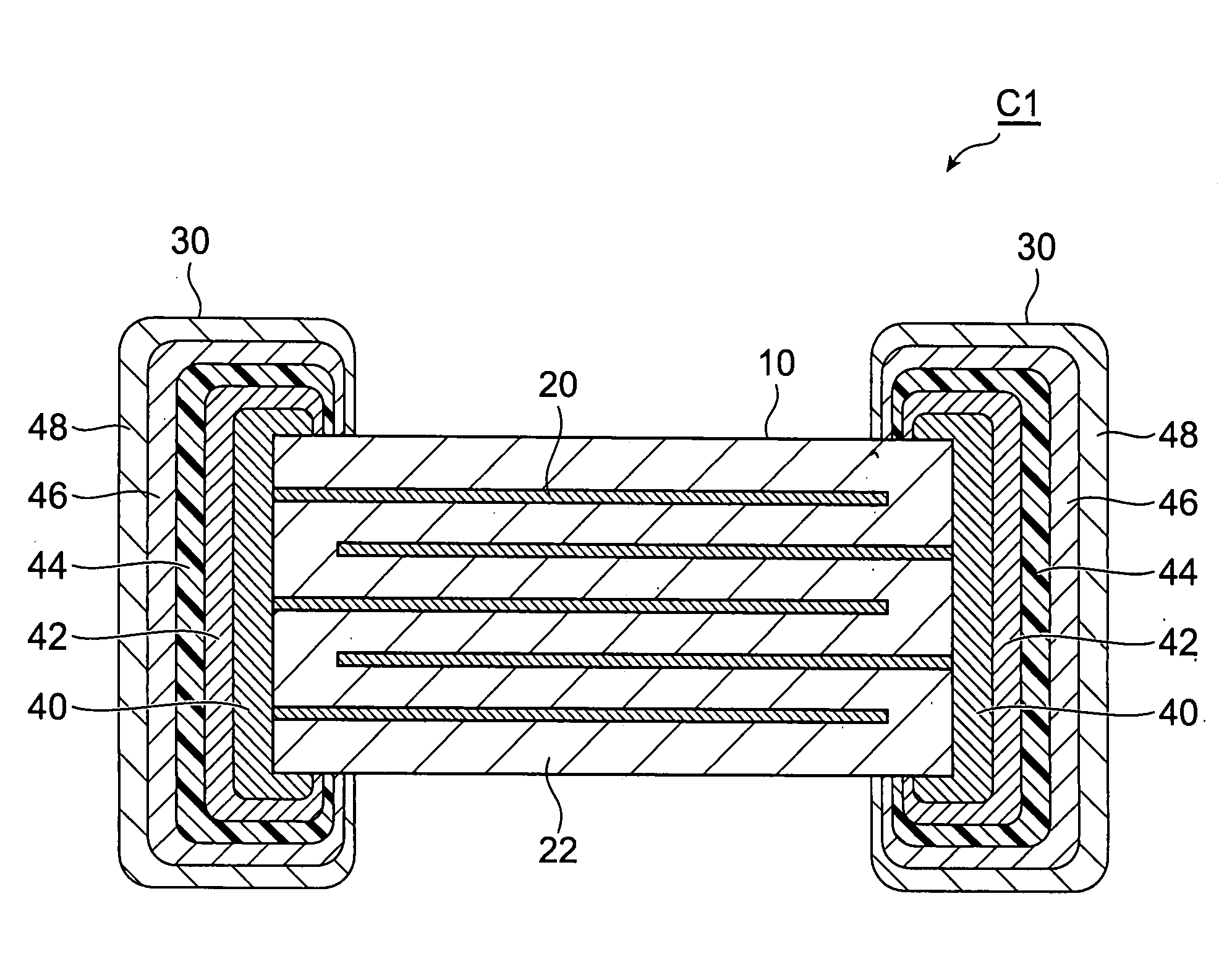
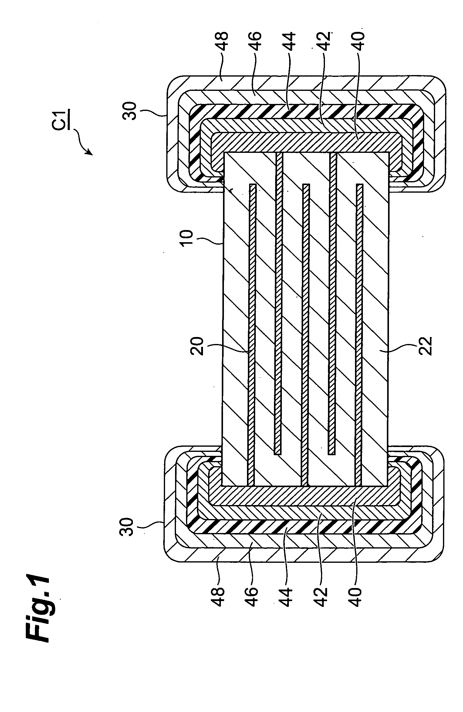
[0023]FIG. 1 is a sectional view of a multilayer capacitor C1 according to an embodiment. The multilayer capacitor C1 has a ceramic sintered body 10, and two external electrodes 30, as shown in FIG. 1.

[0024] In the ceramic sintered body 10, internal electrodes 20 are laminated with dielectric layers 22 in between. The ceramic sintered body 10 is a multilayer body in which the dielectric layers 22 and internal electrodes 20 are alternately laminated. In the actual multilayer capacitor C1, the dielectric layers 22 are integrally formed so that no boundary is visually recognized between dielectric layers 22. The internal electrodes 20 disposed in the ceramic sintered body 10 are alternately drawn ou...


PUM


Abstract

A multilayer capacitor comprises a ceramic sintered body, an internal electrode disposed in the ceramic sintered body, and an external electrode disposed on an external surface of the ceramic sintered body. The external electrode has a first electrode layer formed on the external surface of the ceramic sintered body, a second electrode layer formed on the first electrode layer, and a conductive resin layer formed on the second electrode layer. The internal electrode and the first electrode layer consist primarily of a base metal. The second electrode layer consists primarily of a noble metal or a noble metal alloy. The conductive resin layer contains a noble metal or a noble metal alloy as a conductive material.

Description

BACKGROUND OF THE INVENTION [0001] 1. Field of the Invention [0002] The present invention relates to a ceramic electronic component and a multilayer capacitor. [0003] 2. Related Background Art [0004] Examples of the known ceramic electronic components of this type include those having external electrodes with a resin layer (e.g., Patent Documents 1-4). [0005] A ceramic electronic component of this type is mounted on a substrate by soldering the external electrodes to the substrate in general. When the substrate with the ceramic electronic component thereon is subjected to a thermal shock due to a sudden temperature change, the ceramic electronic component and substrate expand and contract according to their respective coefficients of thermal expansion. On that occasion, the ceramic electronic component and the substrate have different amounts of expansion and contraction due to the difference between the coefficients of thermal expansion, so as to cause deflection. This deflection c...

Claims


Application Information

Patent Timeline
IPC IPC(8): H01G4/06
CPCH01G4/2325
Inventor YOSHII, AKITOSHIAHIKO, TAISUKETAKEDA, ATSUSHIOOTSUKI, SHIROUONODERA, SHINYAKIMURA, MIKIKIKUCHI, HIROMI
Owner TDK CORPARATION
Why Eureka
Try Eureka