Four-transistor Schmitt trigger inverter

Inactive Publication Date: 2006-08-24
SHARP KK
View PDF15 Cites 18 Cited by
  • Summary
  • Abstract
  • Description
  • Claims
  • Application Information

AI Technical Summary

Benefits of technology

[0014] The present invention is a novel Schmitt trigger inverter circuit, employing dual-gate (DG) thin-film transistors (TFTs). The invention's architecture requires only 4 transistors and no other elements, instead of the 6 transistors conventionally required (see FIG. 3). Consequently, more compact circuit implementations, with better area utilization are possible. Also, due to a lower transistor count, lower power dissipation can be obtained than is possible with conventional Schmitt trigger designs. Since many circuits incorporate a large numbers of Schmitt triggers, the benefits of this approach are substantial.

Problems solved by technology

Problems can arise when digital signals are interfaced with circuitry, especially if the digital input signals are corrupted by noise.
This undesirable situation propagates noise artifacts through the interface.

Method used


Image

  • Four-transistor Schmitt trigger inverter
  • Four-transistor Schmitt trigger inverter
  • Four-transistor Schmitt trigger inverter

Examples


Embodiment Construction

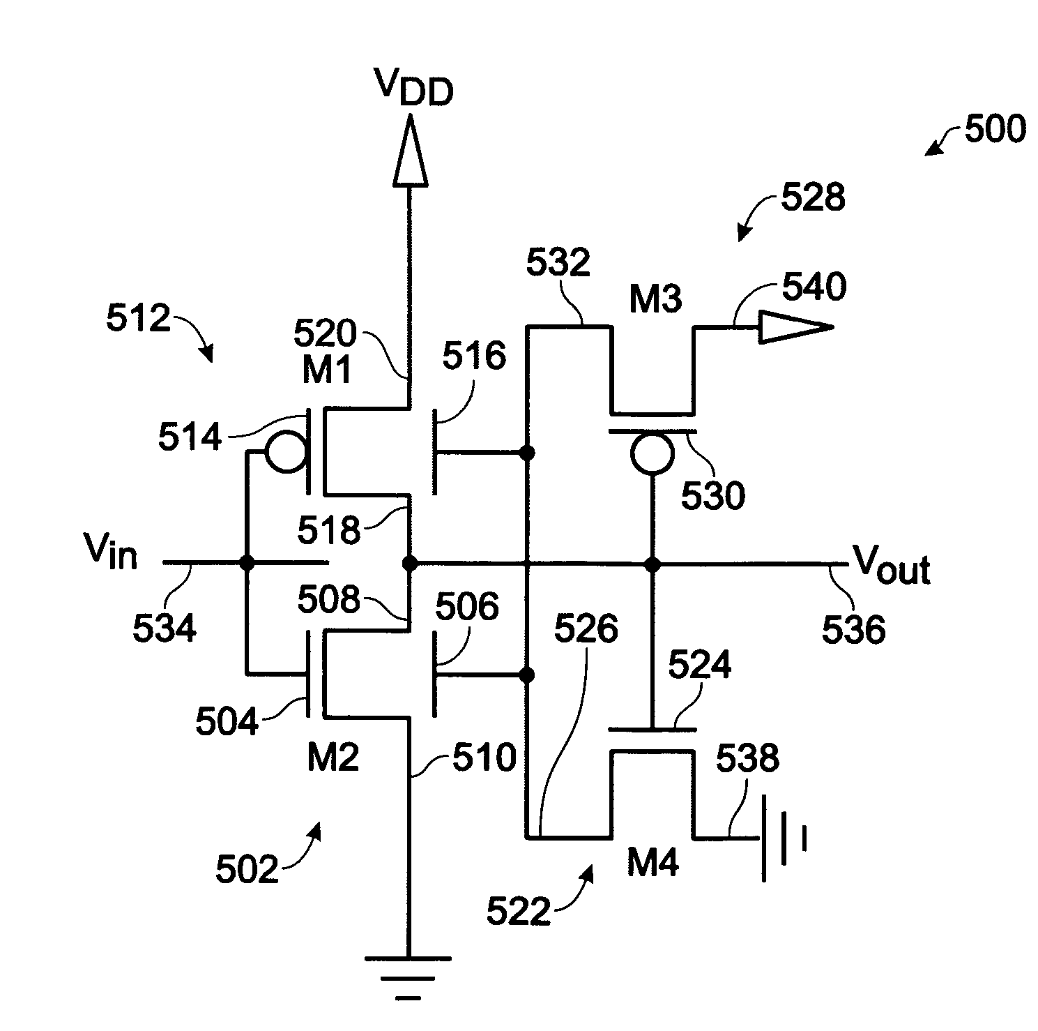
[0031]FIG. 5 is a schematic diagram of a four-transistor Schmitt trigger inverter. The Schmitt trigger inverter 500 comprises a NMOS dual-gate thin-film transistor (DG-TFT) 502 (M2) having a top gate 504, a back gate 506, and source / drain regions 508 and 510. A PMOS DG-TFT 512 (M1) has a top gate 514, a back gate 516, and S / D regions 518 and 520. A NMOS TFT 522 (M4) has a gate 524 connected to an NMOS DG-TFT first S / D region 508 and a PMOS DG-TFT first S / D region 518. The NMOS TFT 522 has a first S / D region 526 connected to the NMOS DG-TFT back gate 506 and the PMOS DG-TFT back gate 516. A PMOS TFT 528 (M3) has a gate 530 connected to the NMOS TFT gate 524, and a first S / D region 532 connected to the NMOS TFT first S / D region 526.

[0032] The NMOS DG-TFT top gate 504 is connected to the input signal (Vin) on line 534 and the first S / D region 508 supplies an output signal (Vout) on line 536. The PMOS DG-TFT top gate 514 is also connected to the input signal on line 534. The NMOS DG-TF...


PUM


Abstract

A four-transistor Schmitt trigger inverter is provided. The Schmitt trigger inverter is made from an n-channel MOS (NMOS) dual-gate thin-film transistor (DG-TFT) and a p-channel MOS (PMOS) DG-TFT, both DG-TFTs having a top gate, a back gate, and source / drain regions. A (conventional) NMOS TFT has a gate connected to an NMOS DG-TFT first S / D region and a PMOS DG-TFT first S / D region. The NMOS TFT also has a first S / D region connected to the NMOS DG-TFT back gate and the PMOS DG-TFT back gate. A (conventional) PMOS TFT has a gate connected to the NMOS TFT gate, and a first S / D region connected to the NMOS TFT first S / D region.

Description

RELATED APPLICATIONS [0001] This application is a continuation-in-part of a pending patent application entitled, MULTI-PLANAR LAYOUT VERTICAL THIN-FILM TRANSISTOR INVERTER, Schuele et al., Ser. No. 10 / 862,761, filed Jun. 7, 2004, Attorney Docket No. SLA0875, which is a continuation-in-part of an issued patent application entitled, VERTICAL THIN FILM TRANSISTOR, invented by Schuele et al., U.S. Pat. No. 6,995,053, filed Apr. 23, 2004, Attorney Docket No. SLA0874. [0002] This application is a continuation-in-part of a pending patent application entitled, DUAL-GATE THIN-FILM TRANSISTOR, invented by Schuele et al., Ser. No. 10 / 953,913, filed Sep. 28, 2004, Attorney Docket No. SLA0909. [0003] This application is a continuation-in-part of a pending patent application entitled, DUAL-GATE TRANSISTOR DISPLAY, invented by Afentakis et al., Ser. No. 11 / 184,699, filed Jul. 18, 2005, Attorney Docket No. SLA8010. [0004] This application is a continuation-in-part of a pending patent application en...

Claims


Application Information

Patent Timeline
IPC IPC(8): H01L21/84H01L29/94
CPCH01L29/78624H01L29/78642H01L29/78648H03K3/3565
Inventor AFENTAKIS, THEMISTOKLESVOUTSAS, APOSTOLOS T.SCHUELE, PAUL J.
Owner SHARP KK
Why Eureka
Try Eureka