Body-biased enhanced precision current mirror

a current mirror and body bias technology, applied in the field of current reference integrated circuits, can solve the problems of mos transistors being imperfect current sources, limited to low current applications, and mos transistors offering a wide dynamic range, so as to increase the output impedance of mos current sources without significant penalty in circuit area or additional margin in operating voltage. , the effect of increasing the output impedance of mos current sources

Inactive Publication Date: 2006-08-31
IBM CORP
View PDF19 Cites 13 Cited by
  • Summary
  • Abstract
  • Description
  • Claims
  • Application Information

AI Technical Summary

Benefits of technology

[0010] A first aspect of the invention is directed to a technique for increasing the output impedance of a MOS current source without significant penalty in circuit area or increase in operating voltage. A current mirror circuit is disclosed with a body-bias voltage adjustment capability to compensate for the effect of a change in output voltage on the output current. For each instance of the current mirror, this approach has the advantage of requiring no additional margin in operating voltage nor does it consume more circuit area than prior art current mirror designs. In addition, the body-enhanced current mirror provides a stable reference current to output current ratio over a wide operating range.

Problems solved by technology

Such current-mirror sensing techniques offer a wide dynamic range, but are generally limited to low current applications.
However, MOS transistors are rendered imperfect current sources because a voltage applied to the drain—typically the output when the transistor is used as a current source—causes a modulation of the size of the drain-channel depletion region.
As a result, the drain current increases as well, hence degrading operation of the device as a constant current source.
However, this technique suffers from either an increase in area with the square of the increase in Leff (since Weff needs to increase by the same proportion) or an increase of the voltage bias margin required for the current source to operate properly in the saturation region.
Unfortunately, this technique has the disadvantage of requiring additional circuit area and an additional voltage drop across the aggregate mirror structure (the mirror and cascode devices) in order for the cascode device to function properly.

Method used


Image

  • Body-biased enhanced precision current mirror
  • Body-biased enhanced precision current mirror
  • Body-biased enhanced precision current mirror

Examples


first embodiment

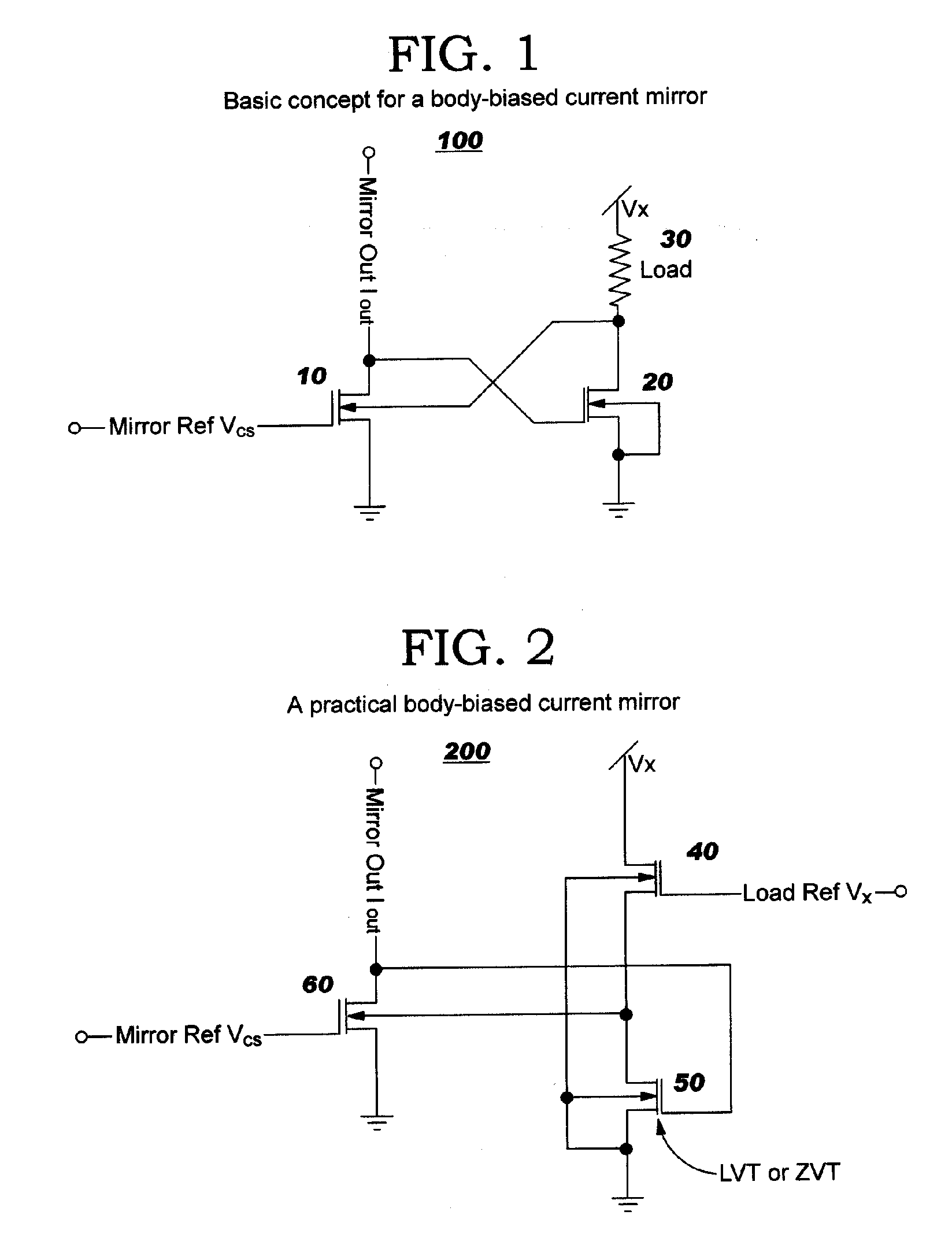
[0021] Referring to FIG. 1, a body-biased current mirror 100 is shown. The drain voltage of NFET current mirror device 10 is monitored by NFET amplifier 20. If the drain voltage of NFET current mirror device 10 increases, the monitor NFET amplifier 20 pulls down on the body of NFET current mirror device 10 and the tendency of the mirror current to increase is counteracted by the resultant increase in the threshold voltage of NFET current mirror device 10. This increases the apparent output impedance of NFET current mirror device 10.

[0022] As shown in FIG. 1, resistor 30 is a load element for the body feedback amplifier 20 that is tied to power supply, Vx. While this circuit topology is conceptually feasible, it has a number of disadvantages, such as requiring significantly increased area and additional processing steps to implement the load as a resistor. In addition, the wire biasing the body feedback amplifier to the supply voltage, Vx has to carry whatever current flows through ...

second embodiment

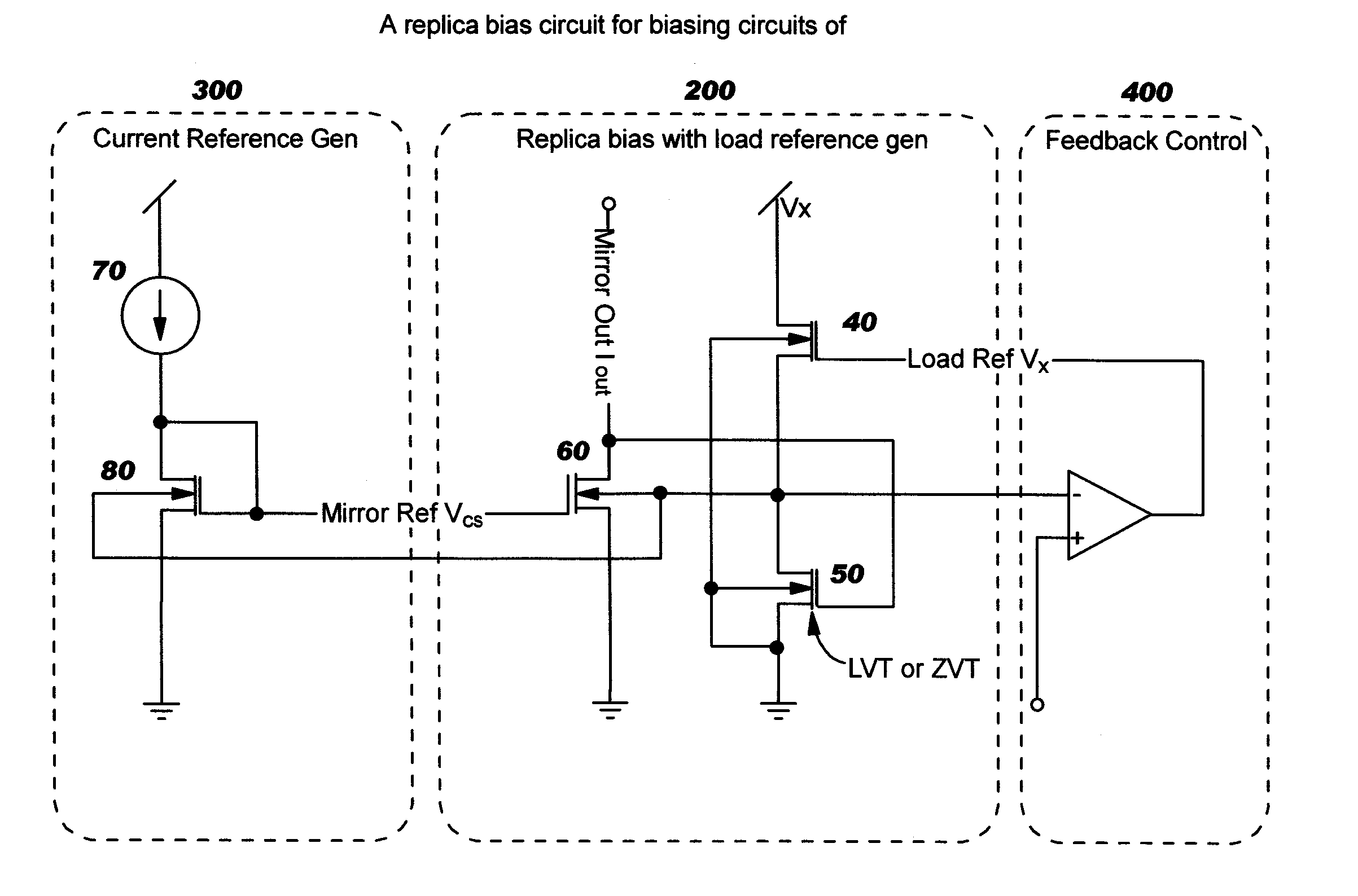
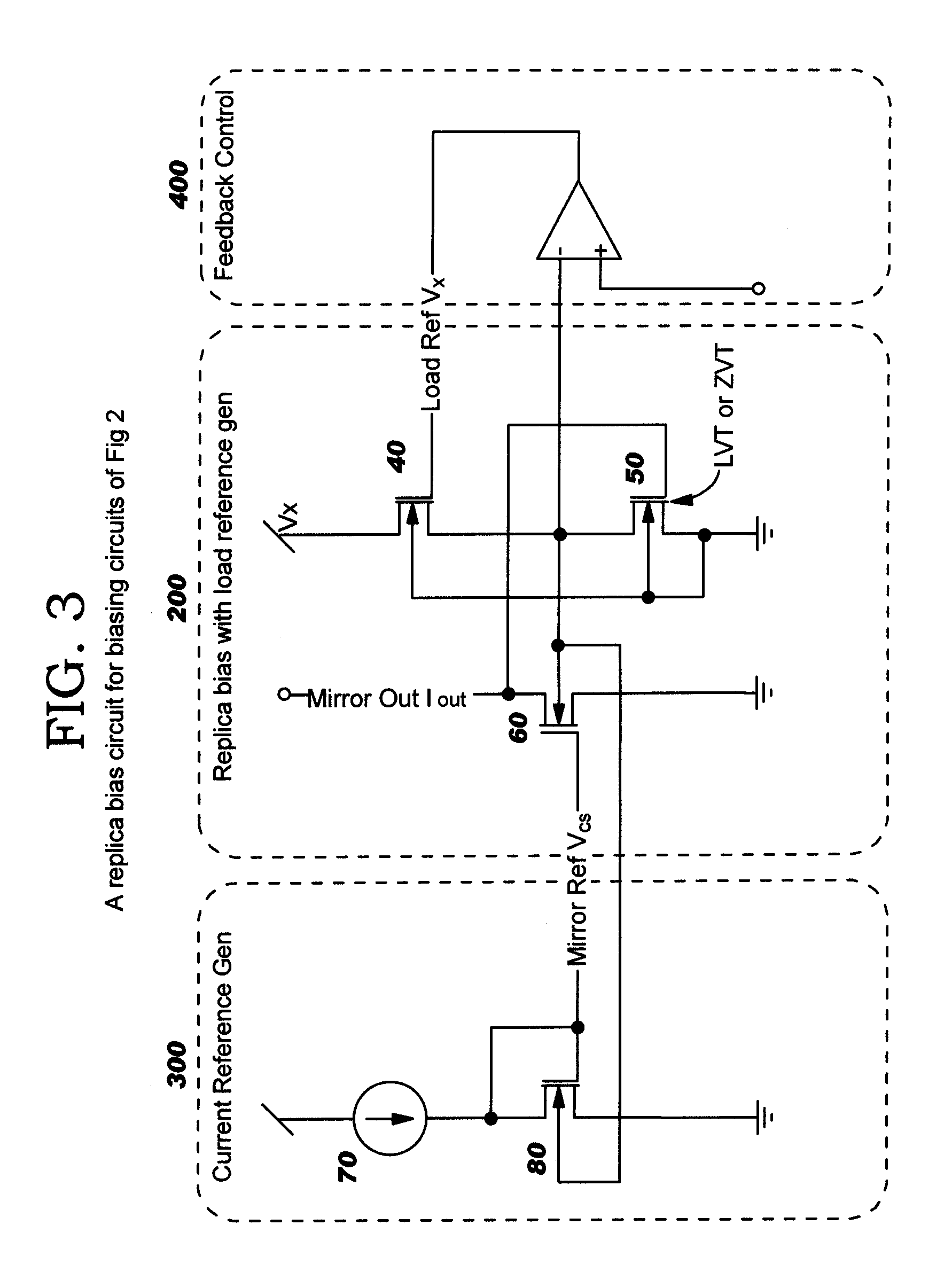
[0023] A smaller and therefore more practical implementation for the current mirror is shown in FIG. 2. In this second embodiment, the load element is represented by MOS load transistor 40 with its gate tied to a reference potential, Vx. Although this circuit operates in the same way as the circuit shown in FIG. 1, the MOS transistor provides a more efficient layout together with more easily controlled design parameters. Another difference is that NFET body feedback amplifier 50 is a low-threshold or zero-threshold transistor, which will turn on in response to very low voltages at the drain of NFET current mirror device 60. As such, the voltage requirement for the mirror is not increased to accommodate the body bias network.

[0024] A circuit for generating the reference voltage Vx is now disclosed. Since the reference voltage may be commonly applied across a large number of current mirror instances, the circuit used to generate this voltage can be somewhat more complex without adding...

third embodiment

[0028] Referring to FIGS. 5-7, a schematic and a set of simulations according to the body-biased enhanced current mirror are shown. In FIG. 5, a second current mirror instance 500 is coupled in parallel to the circuit of FIG. 3. The output current of NFET current mirror device 60 can be made to be decreasing monotonic over the range of interest of its drain voltage by varying the size of the transistors in the mirror reference voltage feedback path. By changing the aspect ratios, and hence the gain in the feedback path, of some of the transistors, the non-monotonic response of the current output may be emphasized or inhibited. More importantly, the non-monotonic behavior of the circuit can be controlled through transistor sizing, so that an optimal response is realized for the body-biased enhanced current mirror.

[0029]FIG. 5 shows a body-biased enhanced current mirror circuit schematic according to a third embodiment, wherein an auxiliary NFET current mirror device 115 is added with...


PUM


Abstract

A body-biased enhanced current mirror reference circuit is disclosed wherein the body bias voltage of a current mirror device is varied to adjust its threshold voltage. Both the drain and body potentials of a replica mirror transistor are controlled to selected values. The drain is set to an expected DC voltage output of an NFET current mirror device. The body potential is set to a maximum desired value to prevent forward biasing of the body-to-diffusion junction(s) of one or more current mirror devices, which is accomplished by a feedback control circuit. A low-frequency, low-precision op amp drives the gate of a replica load device so that the body of the replica NFET current mirror device is set to a maximum bias voltage. The maximum bias voltage is also used to bias the body of a diode connected NMOS reference transistor, so that the current in the NFET current mirror device will be approximately equal to the current in the diode-connected NMOS reference. An auxiliary NFET current mirror device may be added to the body-biased enhanced current mirror circuit with the body connected to ground as in the unmodified current mirror to negate a non-monotonicity of the current output.

Description

FIELD OF THE INVENTION [0001] The field of the invention relates to a current reference integrated circuit and more particularly to a current reference circuit incorporating a biasing scheme to modulate the threshold voltage of an output device of a current mirror to compensate for the effect of a change in output voltage on the output current. BACKGROUND OF THE INVENTION [0002] A MOSFET current mirror is an essential component of integrated circuit amplifiers that is used to implement current sources for biasing and may also operate as an active load. The MOSFET current mirror typically includes at least two devices configured such that the ratio of currents through each device remains largely constant. The current ratio is controlled by the physical geometry of the transistors, which enables the current flowing through a larger device to be approximated by reference to the current flowing through a smaller device. In this regard, current in the larger device can be measured by a p...

Claims


Application Information

Patent Timeline
Patent Type & Authority Applications(United States)
IPC IPC(8): G05F1/10
CPCG05F3/262
Inventor BONACCIO, ANTHONY R.CRANFORD, HAYDEN C. JR.
Owner IBM CORP
Why Eureka
Try Eureka