Chip structure and manufacturing process thereof

Inactive Publication Date: 2006-09-07
ADVANCED SEMICON ENG INC
View PDF1 Cites 5 Cited by
  • Summary
  • Abstract
  • Description
  • Claims
  • Application Information

AI Technical Summary

Benefits of technology

[0008] The object of the present invention is to provide a chip structure and manufacturing process thereof, in which an improved passiva

Problems solved by technology

Because moistures easily infiltrate into the chip structure from the cuts, delamination

Method used


Image

  • Chip structure and manufacturing process thereof
  • Chip structure and manufacturing process thereof
  • Chip structure and manufacturing process thereof

Examples


Embodiment Construction

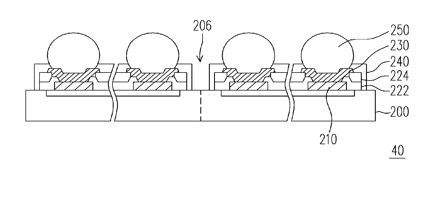
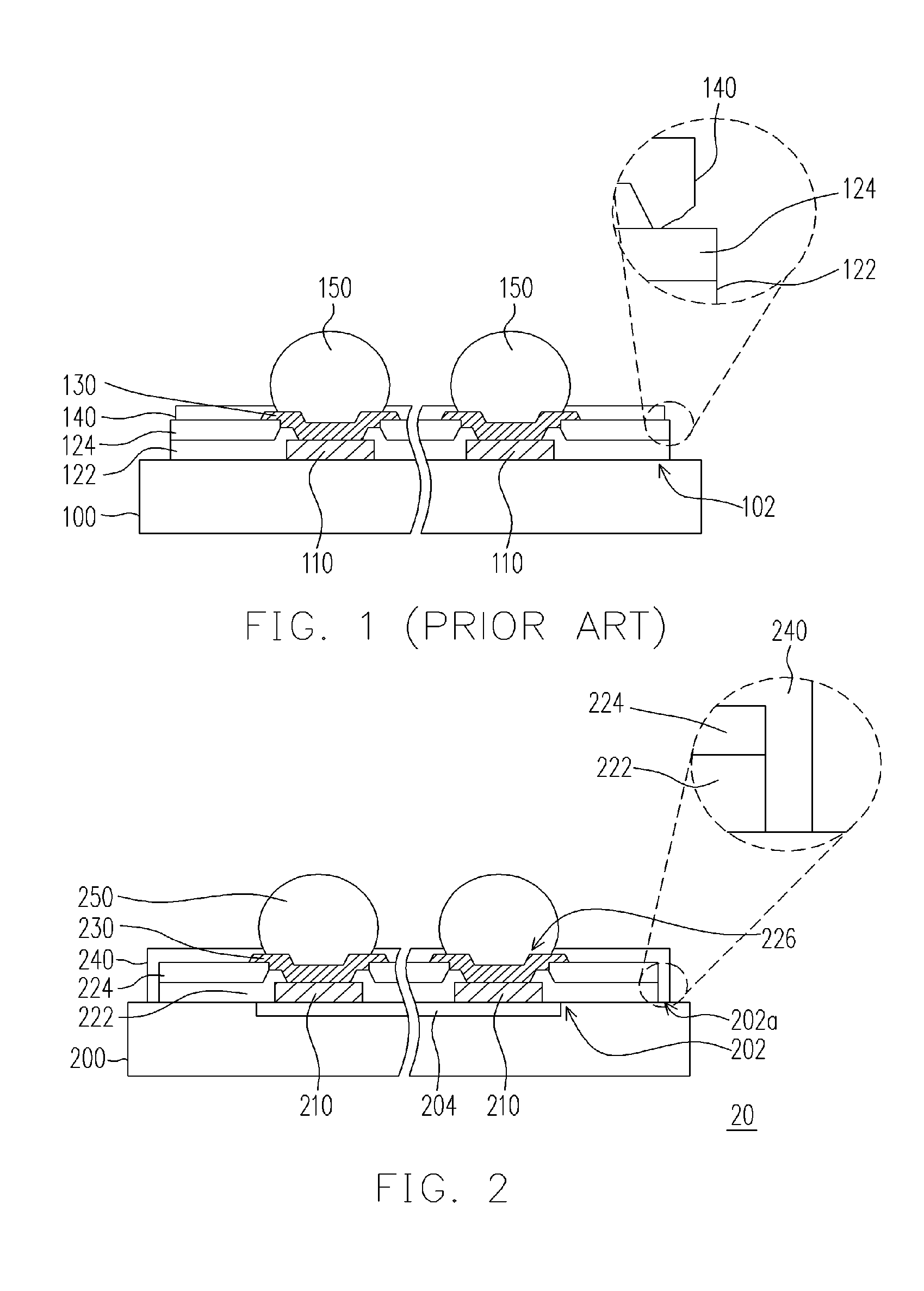
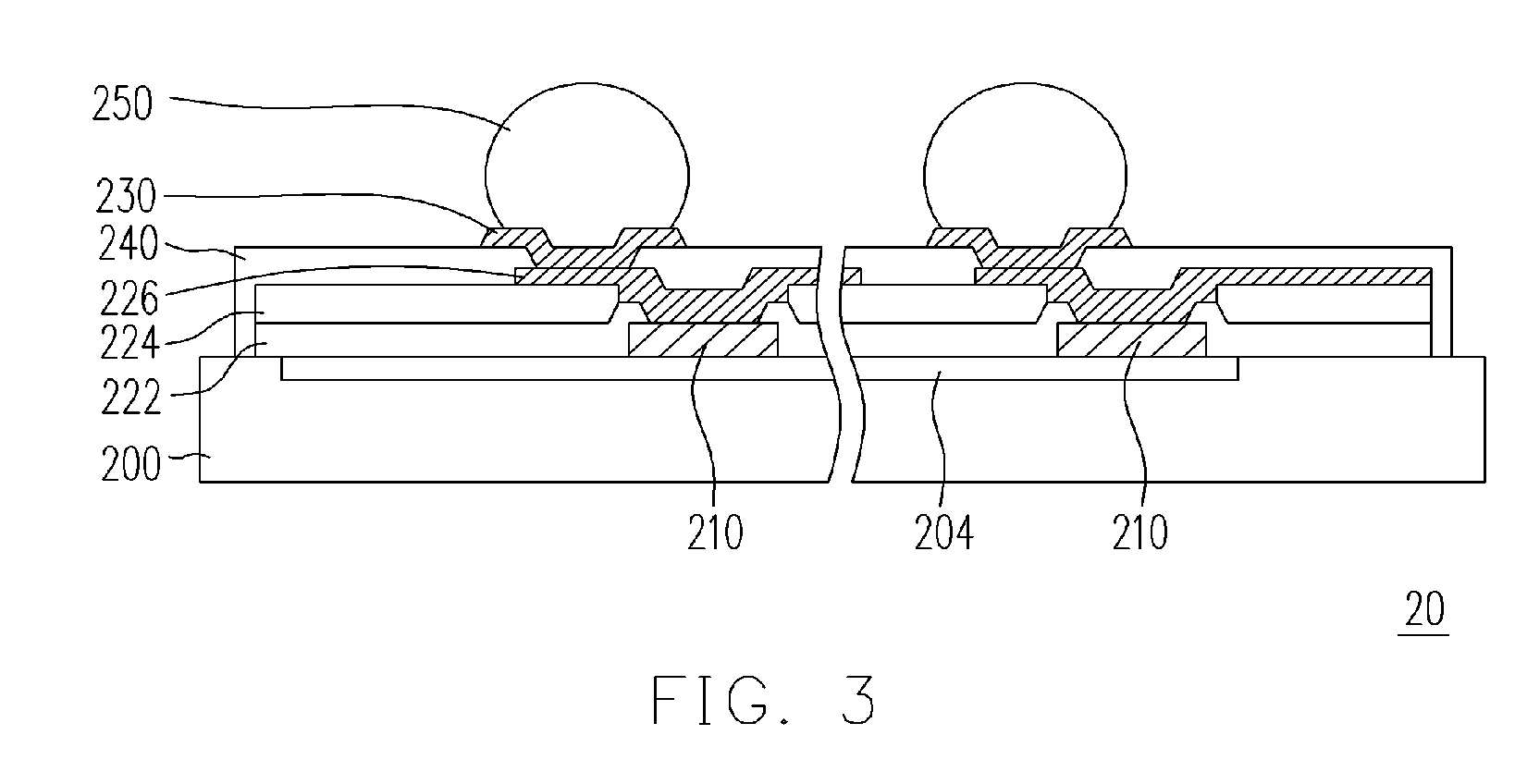
[0022] Referring to FIG. 2, it is a schematic partial cross-sectional view of a chip structure in a preferred embodiment of the present invention. In the present embodiment, the chip structure 20 mainly comprises a substrate 200, a plurality of bonding pads 210, a first passivation layer 224, a plurality of under ball metal layers 230 and a second passivation layer 240. The substrate (e.g. silicon) 200 has at least a circuitry unit 204 including IC layouts. The circuitry unit 204 is located in the substrate 200, and bonding pads 210 are disposed on an active surface 202 of the substrate 200. Each of the bonding pads 210 is disposed on the circuitry unit 204 and electrically connected to the ICs. Furthermore, the first passivation layer 224 is formed on the active surface 202 of the substrate 200. Then, a portion of the first passivation layer 224 is removed through a patterning process, such that each of the bonding pads 210 and a portion of the active surface 202a are exposed by th...


PUM


Abstract

A chip structure and the manufacturing process thereof are provided. The feature of the present application is that the chip structure has a first passivation layer covering a substrate of the chip and exposing each of bonding pads and a portion of the substrate surface, and a second passivation layer covering the sidewalls of the first passivation layer and the portion of substrate surface exposed by the first passivation layer, to prevent moisture infiltration from the edge of the substrate. Therefore, the reliability of the chip structure is enhanced.

Description

CROSS-REFERENCE TO RELATED APPLICATION [0001] This application claims the priority benefit of Taiwan application serial no. 94104991, filed on Feb. 21, 2005. All disclosure of the Taiwan application is incorporated herein by reference. BACKGROUND OF THE INVENTION [0002] 1. Field of Invention [0003] The present invention relates to a chip structure. More particularly, the present invention relates to a chip structure having a plurality of passivation layers and the manufacturing process thereof. [0004] 2. Description of Related Art [0005] In the semiconductor industry, the manufacture of the integrated circuits (ICs) can mainly be categorized as three stages: the manufacture of wafers, the manufacture of the ICs and the packaging of the ICs. Furthermore, the dies are formed following the steps of wafer manufacturing, circuit designing, circuit manufacturing and wafer cutting. In general, each of the dies includes a passivation layer covering the surface of the silicon substrate and e...

Claims


Application Information

Patent Timeline
IPC IPC(8): H01L21/00H01L23/02
CPCH01L23/3171H01L24/10H01L2224/13099H01L2924/14H01L24/13H01L2924/00H01L2924/351H01L2224/13H01L2224/05022H01L2224/05001H01L2224/05572H01L2224/056H01L2924/00014H01L24/05H01L2224/05099
Inventor TSAI, MON-CHINLO, JIAN-WENFU, SHAO-WENWANG, CHI-YU
Owner ADVANCED SEMICON ENG INC
Why Eureka
Try Eureka