

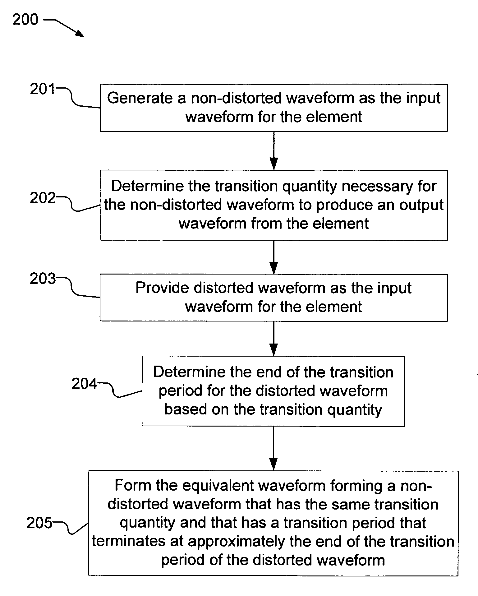
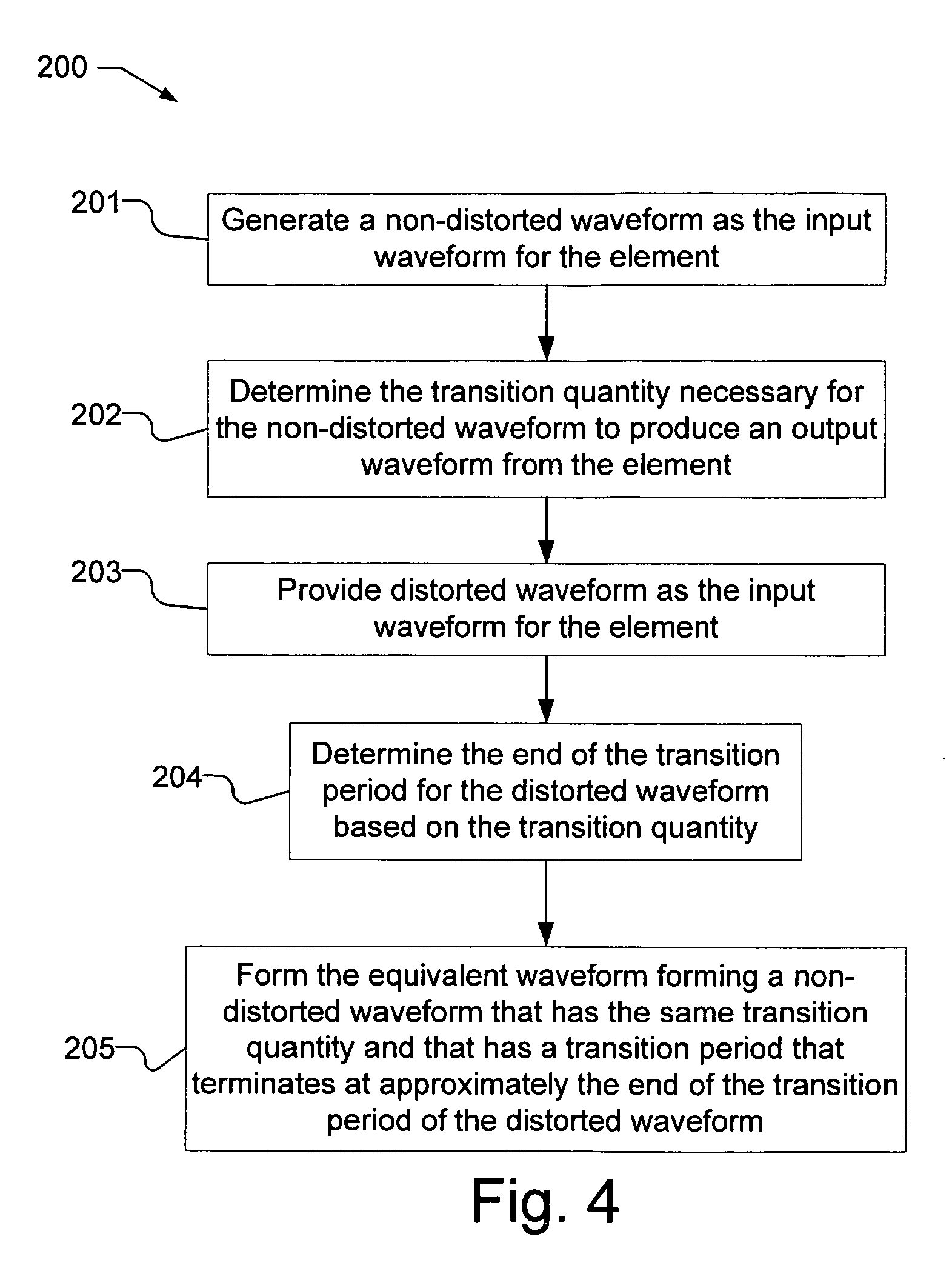
Determining equivalent waveforms for distorted waveforms
a technology of equivalent waveforms and distorted waveforms, applied in error detection/correction, program control, instruments, etc., can solve the problems of clock frequency, timing and signal integrity errors, and the source of device geometry and desired power consumption, so as to achieve accurate equivalent waveforms and obtain them quickly
- Summary
- Abstract
- Description
- Claims
- Application Information
AI Technical Summary
Benefits of technology
Problems solved by technology
Method used
Image

Examples
Embodiment Construction
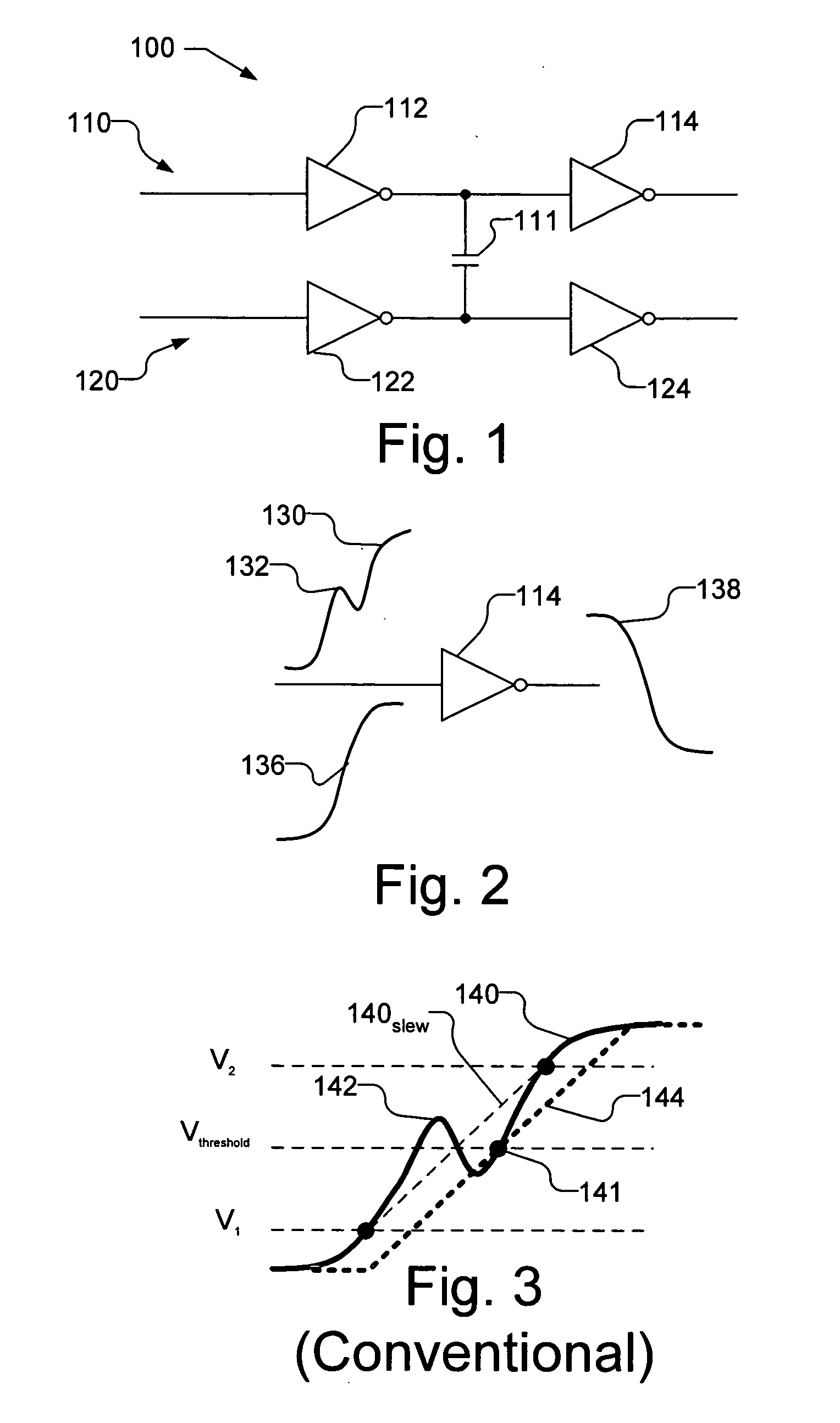
[0020]FIG. 1 schematically illustrates an example of a cross coupled circuit 100 that may have its timing analyzed using an equivalent waveform that is produced in accordance with an embodiment of the present invention. The cross coupled circuit 100 includes a primary line 110 that is coupled to an aggressor line 120 through cross coupling capacitance, shown as capacitor 111. The primary line 110 is illustrated as including an inverter 112 coupled to a second inverter 114 and the aggressor line 120 is similarly illustrated as an inverter 122 coupled to a second inverter 124. It should be understood that the cross coupled circuit 100 is merely exemplary and that the present invention may be used advantageously with any circuit that suffers from waveform distortion due to various reasons including, but not limited to, capacitive coupling, inductive coupling, inductive ringing, and resistive shielding effects.
[0021] Generally, each node in the cross coupled circuit 100 includes a self...
PUM
 Abstract
Description
Claims
Application Information